Samsung K4M511533E - Y(П)C L F Data Handbook
Summary
This high-performance Mobile SDRAM module provides superior data storage for demanding applications. The technical manual offers comprehensive details essential for integration, including functional block diagrams, absolute maximum ratings, detailed power-up sequences, and optimal operating conditions. It supports advanced features like Partial Array Self Refresh (PASR) and DQM masking. This component is specifically engineered for hardware engineers developing mobile, telecommunications, and high bandwidth portable electronic devices that require reliable, compact memory solutions.
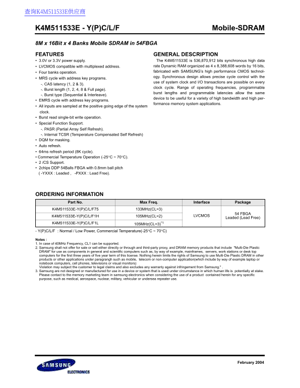
Page 1 Text Content
K4M511533E - Y(P)C/L/F Mobile-SDRAM 8M x 16Bit x 4 Banks Mobile SDRAM in 54FBGA FEATURES GENERAL DESCRIPTION • 3.0V or 3.3V power supply. The K4M511533E is 536,870,912 bits synchronous high data
• LVCMOS compatible with multiplexed address. rate Dynamic RAM organized as 4 x 8,388,608 words by 16 bits, fabricated with SAMSUNG’s high performance CMOS technol-
• Four banks operation.
ogy. Synchronous design allows precise cycle control with the
• MRS cycle with address key programs.
use of system clock and I/O transactions are possible on every
-. CAS latency (1, 2 & 3).
clock cycle. Range of operating frequencies, programmable
-. Burst length (1, 2, 4, 8 & Full page).
burst lengths and programmable latencies allow the same
-. Burst type (Sequential & Interleave).
device to be useful for a variety of high bandwidth and high per-
• EMRS cycle with address key programs.
formance memory system applications.
• All inputs are sampled at the positive going edge of the system clock. • Burst read single-bit write operation. • Special Function Support. -. PASR (Partial Array Self Refresh). -. Internal TCSR (Temperature Compensated Self Refresh) • DQM for masking. • Auto refresh. • 64ms refresh period (8K cycle). • Commercial Temperature Operation (-25°C ~ 70°C). • 2 /CS Support. • 2chips DDP 54Balls FBGA with 0.8mm ball pitch ( -YXXX : Leaded , -PXXX : Lead Free).
ORDERING INFORMATION
Part No. Max Freq. Interface Package
K4M511533E-Y(P)C/L/F75 133MHz(CL=3)
54 FBGA
105MHz(CL=2) LVCMOS
Leaded (Lead Free)K4M511533E-Y(P)C/L/F1H
105MHz(CL=3)*1
- Y(P)C/L/F : Normal / Low Power, Commercial Temperature(-25°C ~ 70°C)
Notes : 1. In case of 40MHz Frequency, CL1 can be supported. 2. Samsung shall not offer for sale or sell either directly or through and third-party proxy, and DRAM memory products that include "Multi-Die Plastic DRAM" for use as components in general and scientific computers such as, by way of example, mainframes, servers, work stations or desk top computers for the first three years of five year term of this license. Nothing herein limits the rights of Samsung to use Multi-Die Plastic DRAM in other products or other applications under paragrangh such as mobile, telecom or non-computer application(which include by way of example laptop or notebook computers, cell phones, televisions or visual monitors) Violation may subject the customer to legal claims and also excludes any warranty against infringement from Samsung." . 3. Samsung are not designed or manufactured for use in a device or system that is used under circumstance in which human life is potentially at stake. Please contact to the memory marketing team in samsung electronics when considering the use of a product contained herein for any specific purpose, such as medical, aerospace, nuclear, military, vehicular or undersea repeater use.
February 2004
Page Summary Contents For Samsung K4M511533E - Y(П)C L F Data Handbook
Manual Details
| Brand | Samsung |
|---|---|
| Pages | 12 |
| File Size | 104.89 KB |
| Published | June 17, 2026 |
Enter the captcha to get the download link:

Frequently Asked Questions
What voltage is required for VDD and VDDQ?
The recommended operating range for both VDD and VDDQ is between 2.7V and 3.6V.
How does the device handle memory refresh cycles?
It supports Auto refresh and has a 64ms refresh period (8K cycle). It also features Partial Array Self Refresh (PASR) and Internal TCSR.
What is the recommended minimum power-up sequence for operation?
The required steps include applying VDD before or with VDDQ, maintaining stable clock/power for 200us, issuing precharge commands, auto-refresh commands, and mode register set commands.
Is this DDR memory designed for critical systems?
No. The manual states that the device is not designed or manufactured for use in a system where human life could be potentially at stake (e.g., medical, aerospace).
What maximum storage temperature can the module withstand?
The recommended operating condition for Storage Temperature range (TSTG) is -55 to +150°C.