ROHM VT6T1 User Guide and Manual
Summary
This compact VT6T1 dual transistor unit is an essential power management component built for reliable switching and LED driving applications. Detailed documentation provides electrical characteristics, absolute maximum ratings, and application guides needed by electronics engineers and circuit designers. Whether you are designing a new switcher or optimizing driver circuits, this manual offers all the necessary technical specifications to ensure accurate product implementation.
Page 1 Text Content
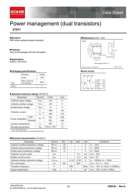
Power management (dual transistors) VT6T1 Structure Dimensions (Unit : mm) PNP silicon epitaxial planar transistor
Features 0 ~ 0.05 Very small package with two transistors.
Applications
Switch, LED driver
Abbreviated symbol : T1
Each lead has same dimensions. UNIT : mm
Packaging specifications Inner circuit
Package Taping
Code T2R
(1) Emitter (Tr1)
Basic ordering
(2) Base (Tr1)
Tr2Tr1
Type unit (pieces) (3) Collector (Tr2)
(4) Emitter (Tr2)
VT6T1 (5) Base (Tr2)
(1) (3)(2) (6) Collector (Tr1)
Absolute maximum ratings (Ta=25°C)
Parameter Symbol Limits Unit
Collector-base voltage VCBO −20 Collector-emitter voltage VCEO −20 Emitter-base voltage VEBO −5 IC m A−200
Collector current
ICP m A−400 0. .1 0. .1
Total m W
∗2 Power dissipation PD
Element m W
Junction temperature Tj °C
Storage temperature Tstg −55 to +150 °C
∗1 Pw=1m S Single pulse ∗2 Each terminal mounted on a recommended land
Electrical characteristics (Ta=25°C)
Parameter Symbol Min. Typ. Max. Unit Conditions
Collector-emitter breakdown voltage BVCEO −20 IC= −1m A
Collector-base breakdown voltage BVCBO −20 IC= −50µA
Emitter-base breakdown voltage BVEBO −5 IE= −50µA Collector cut-off current ICBO −0.1 µA VCB= −20V Emitter cut-off current IEBO −0.1 µA VEB= −5V Collector-emitter saturation voltage VCE(sat) −0.12 −0.30 IC= −100m A, IB= −10m A
DC current gain h FE VCE= −2V, IC= −1m A Transition frequency f T MHz VCE= −10V, IE=10m A, f=100MHz Cob p F VCB= −10V, IE=0A, f=1MHz Output capacitance
1/2 www.rohm.com 2009.06 - Rev.A
○c 2009 ROHM Co., Ltd. All rights reserved.
Page Summary Contents For ROHM VT6T1 User Guide and Manual
Manual Details
| Brand | ROHM |
|---|---|
| Pages | 3 |
| File Size | 187.48 KB |
| Published | May 31, 2026 |
Enter the captcha to get the download link:

Frequently Asked Questions
What is the overall temperature range for operation of this transistor?
The junction temperature (Tj) ranges from -55 to +150°C.
How much power can the device dissipate in total?
The total maximum power dissipation (PD) is specified as 150 mW.
What is the recommended application for this dual-transistor unit?
It is suitable for applications such as switches and LED drivers.
Can I use this product in mission-critical or life support equipment?
No, it should not be used for equipment requiring an extremely high level of reliability, such as medical instruments or aerospace machinery.