ROHM VT6M1 User Guide and Manual
Summary
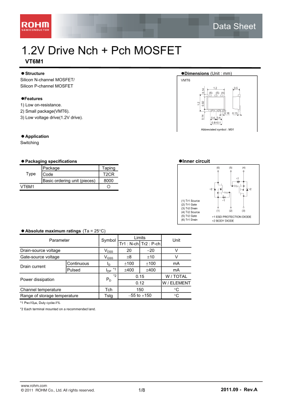
The VT6M1 is a complementary pair of 1.2V-drive N-channel and P-channel MOSFETs in a compact VMT6 package. Features include low on-resistance, small footprint, and low voltage drive capability. The N-channel device handles 20V drain-source voltage with ±100mA continuous current, while the P-channel supports -20V. Both devices feature ±8V to ±10V gate-source ratings and 150°C channel temperature. Applications include switching circuits where space and low-voltage control are critical. Target users are electronics engineers and PCB designers developing compact battery-powered devices, portable electronics, and low-voltage switching applications.
Page 1 Text Content
Data Sheet
1.2V Drive Nch + Pch MOSFET VT6M1 Structure Dimensions (Unit : mm) Silicon N-channel MOSFET/ VMT6 Silicon P-channel MOSFET
Features 1) Low on-resistance.
2) Small package(VMT6). (1) (2) (3)
3) Low voltage drive(1.2V drive). 0.4 0.4 0.8±0.1
Abbreviated symbol : M01
Application Switching
Packaging specifications Inner circuit
Package Taping (6) (5) (4)
Type Code T2CR
Basic ordering unit (pieces)
VT6M1
(1) Tr1 Source ∗1
(2) Tr1 Gate (3) Tr2 Drain
(4) Tr2 Source (5) Tr2 Gate 1 ESD PROTECTION DIODE (6) Tr1 Drain
2 BODY DIODE
Absolute maximum ratings (Ta = 25C)
Limits
Parameter Symbol Unit
Tr1 : N-ch Tr2 : P-ch
Drain-source voltage VDSS 20 Gate-source voltage VGSS 8 10
Continuous ID 100 100 m A
Drain current
Pulsed IDP *1 400 400 m A *2 0.15 W / TOTAL Power dissipation PD
0.12 W / ELEMENT
Channel temperature Tch C
Range of storage temperature Tstg 55 to 150 C
*1 Pw10s, Duty cycle1%
*2 Each terminal mounted on a recommended land.
www.rohm.com
© 2011 ROHM Co., Ltd. All rights reserved. 1/8 2011.09 - Rev.A
Page Summary Contents For ROHM VT6M1 User Guide and Manual
Manual Details
| Brand | ROHM |
|---|---|
| Pages | 9 |
| File Size | 1.29 MB |
| Published | June 16, 2026 |
Enter the captcha to get the download link:

Frequently Asked Questions
What are the key features of the VT6M1 MOSFET?
Low on-resistance, small VMT6 package, and low voltage drive (1.2V).
What is the absolute maximum drain-source voltage for the N-channel part?
The drain-source voltage (VDSS) absolute maximum rating is 20V for the N-channel (Tr1).
What is the typical static on-state resistance for the P-channel at Vgs=-1.5V?
The typical RDS(on) for the P-channel (Tr2) is 13.2 Ω max at I_D = -10mA and V_GS = -1.5V.
What ESD protection is recommended for this MOSFET?
The datasheet advises designing an ESD protection circuit as the product may be vulnerable in large electrified environments.