ROHM SH8M14 User Guide and Manual
Summary
This robust MOSFET package seamlessly combines both N-channel and P-channel FETs, providing a high-power solution for efficient switching applications. This comprehensive technical data sheet is essential reading for electrical engineers and power electronics designers. It details critical operational parameters, including low on-resistance figures, maximum ratings, detailed switching waveforms, gate charge analysis, and thermal resistance curves. Use this guide to ensure optimal integration and reliable performance in your next circuit design.
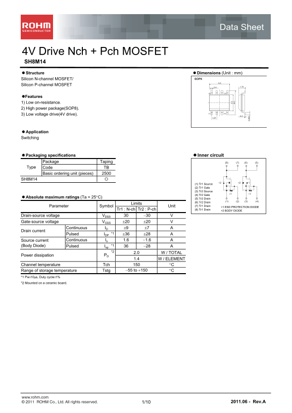
Page 1 Text Content
Data Sheet
4V Drive Nch + Pch MOSFET SH8M14 Structure Dimensions (Unit : mm)
Silicon N-channel MOSFET/ SOP8
Silicon P-channel MOSFET
Features 1) Low on-resistance. 2) High power package(SOP8).
3) Low voltage drive(4V drive).
Application Switching
Packaging specifications Inner circuit
Package Taping (8) (7) (6) (5)
Type Code TB
Basic ordering unit (pieces)
SH8M14
(1) Tr1 Source (2) Tr1 Gate (3) Tr2 Source
(4) Tr2 Gate
Absolute maximum ratings (Ta = 25C)
(5) Tr2 Drain
(6) Tr2 Drain (1) (2) (3) (4)
Limits
Parameter Symbol Unit (7) Tr1 Drain
∗1 ESD PROTECTION DIODE
Tr1 : N-ch Tr2 : P-ch (8) Tr1 Drain
∗2 BODY DIODE
Drain-source voltage VDSS 30
Gate-source voltage VGSS 20 20 Continuous ID 9 7
Drain current
Pulsed IDP *1 36 28
Source current Continuous Is 1.6 1.6
(Body Diode) Pulsed Isp *1 28 *2
2.0 W / TOTAL
Power dissipation PD
1.4 W / ELEMENT
Channel temperature Tch C
Range of storage temperature Tstg 55 to 150 C
*1 Pw10s, Duty cycle1% *2 Mounted on a ceramic board.
www.rohm.com © 2011 ROHM Co., Ltd. All rights reserved. 1/10 2011.06 - Rev.A
Page Summary Contents For ROHM SH8M14 User Guide and Manual
Manual Details
| Brand | ROHM |
|---|---|
| Pages | 11 |
| File Size | 1.22 MB |
| Published | June 18, 2026 |
Enter the captcha to get the download link:

Frequently Asked Questions
What warning is provided regarding electrical environments when using this product?
The notice advises that the product might cause chip aging and breakdown in large electrified environments, recommending an ESD protection circuit design.
What is the minimum recommended mounting surface for optimal operation?
It must be mounted on a ceramic board to ensure proper heat dissipation.
How are the maximum specified drain-source voltage ranges outlined?
The absolute maximum ratings specify V_DSS limits of ±30V for both N-channel (Tr1) and P-channel (Tr2).
What is the typical static on-state resistance range?
For Tr1 (N-ch), it ranges from 18 to 25 mΩ, while for Tr2 (P-ch), it ranges from 29.0 to 39.0 mΩ.