ROHM DTD723YE DTD723YM Data Sheet
Summary
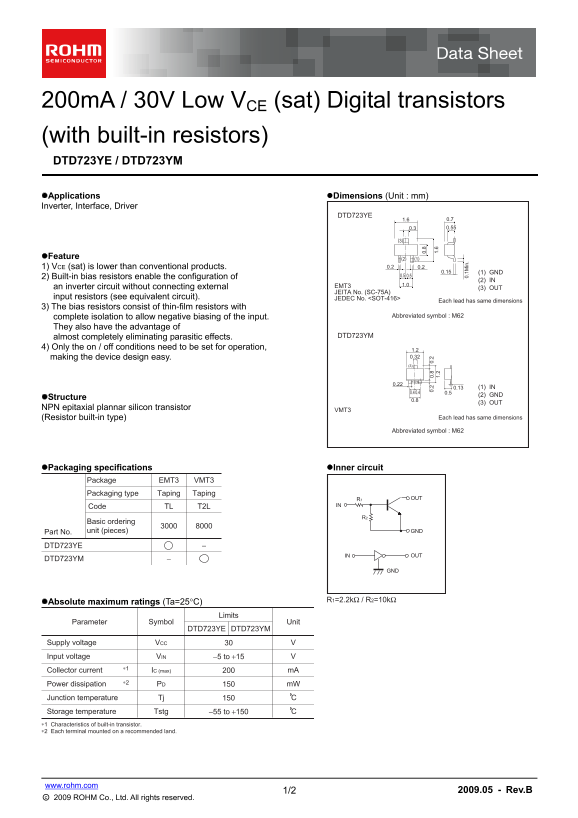
These low voltage digital transistors are optimized for signal interfacing, driving, and inverter applications. Featuring built-in resistors, they significantly simplify circuit design by eliminating external biasing components while maintaining high performance (low Vsat). This guide provides comprehensive technical specifications, including absolute ratings, detailed electrical curves, and structural data, enabling engineers to reliably integrate the device into complex electronic systems for robust signal management.
Page 1 Text Content
200m A / 30V Low VCE (sat) Digital transistors (with built-in resistors) DTD723YE / DTD723YM Applications Dimensions (Unit : mm) Inverter, Interface, Driver
DTD723YE
Feature (2) (1)
1) VCE (sat) is lower than conventional products. 0.2 0.2
0.15 (1) GND
2) Built-in bias resistors enable the configuration of 0.50.5
(2) IN
EMT3 1.0
an inverter circuit without connecting external (3) OUT
JEITA No. (SC-75A)
input resistors (see equivalent circuit). JEDEC No. <SOT-416>
Each lead has same dimensions
3) The bias resistors consist of thin-film resistors with
complete isolation to allow negative biasing of the input. Abbreviated symbol : M62
They also have the advantage of
almost completely eliminating parasitic effects. DTD723YM
4) Only the on / off conditions need to be set for operation,
1.2 making the device design easy. 0.32 (3)
0.13 (1) IN
(2) GND
Structure
(3) OUT
NPN epitaxial plannar silicon transistor
(Resistor built-in type) Each lead has same dimensions
Abbreviated symbol : M62 0. 0. 0.
Packaging specifications Inner circuit 0. 1M in
Package EMT3 VMT3 Packaging type Taping Taping
R1 OUT
Code TL T2L IN
Basic ordering
Part No. unit (pieces) GND
DTD723YE
IN OUT
DTD723YM
Absolute maximum ratings (Ta=25°C)
Limits
Parameter Symbol Unit
DTD723YE DTD723YM
Supply voltage VCC
Input voltage VIN −5 to +15
Collector current IC (max) m A
Power dissipation ∗2 PD m W
Junction temperature Tj
Storage temperature Tstg −55 to +150
∗1 Characteristics of built-in transistor. ∗2 Each terminal mounted on a recommended land.
1/2 www.rohm.com 2009.05 - Rev.B
○c 2009 ROHM Co., Ltd. All rights reserved.
Page Summary Contents For ROHM DTD723YE DTD723YM Data Sheet
Manual Details
| Brand | ROHM |
|---|---|
| Pages | 3 |
| File Size | 178.85 KB |
| Published | June 17, 2026 |
Enter the captcha to get the download link:

Frequently Asked Questions
What is the max collector current of DTD723YE?
The maximum collector current is 200mA at 25°C.
What are the built-in resistor values?
R1 is 2.2kΩ and R2 is 10kΩ.
What packages do these transistors come in?
They come in EMT3 and VMT3 packages.
Is this transistor suitable for medical devices?
No, it is not designed for medical or other high-risk safety devices.