ROHM DTDG23YP Data Sheet
Summary
This comprehensive datasheet details the DTDG23YP NPN planar silicon transistor, a robust switching component ideal for power electronic applications like inverters, interface circuits, and drivers. The manual provides expert engineers with exhaustive specifications, including detailed electrical characteristics, graphs illustrating performance curves, absolute maximum ratings, and application advice. Designed with built-in zener diode protection and high DC current gain, this reliable transistor is engineered for demanding circuit designs requiring stable and efficient switching performance.
Page 1 Text Content
DTDG23YP
Transistors
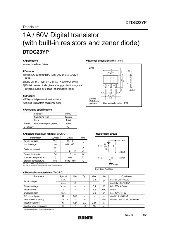
1A / 60V Digital transistor (with built-in resistors and zener diode) DTDG23YP Applications External dimensions (Unit : mm) Inverter, Interface, Driver
Features 1.6 1) High DC current gain. (Min. 300 at VO / IO=2V / 0.5A) 2) Low Vo(on). (Typ. 0.4V at IO / II=500m A / 5m A)
3) Built-in zener diode gives strong protection against (3)(2)(1)
reverse surge by L-load (an inductive load). 0.4
Structure
(1)Base
NPN epitaxial planar silicon transistor
(2)Collector
(with built-in resistors and zener diode) (3)Emitter Abbreviated symbol : E02
Packaging specifications
Package MPT3 Packaging type Taping Code T100
Part No. Basic ordering unit (pieces) 4. 02.
DTDG23YP
Absolute maximum ratings (Ta=25°C) Equivalent circuit Parameter Symbol Limits Unit
Supply voltage VCC 60±10
Input voltage VIN −6 to +40 R1 IN
Collector current R2
ICP A∗1
Power dissipation Pd 1.5 W∗2 Junction temperature Tj IN OUT Storage temperature Tstg −55 to +150 ∗1 Pw 10ms, Duty cycle 2%<−<−
∗2 When mounted on 40 40 0.7mm ceramic board.+
Electrical characteristics (Ta=25°C)
Parameter Symbol Min. Typ. Max. Unit Conditions
VI(off) 0.3 VCC=5V , IO=100µA
Input voltage
VI(on) VO=0.4V , IO=100m A Output voltage VO(on) 0.4 IO/II=500m A/5m A Input current II 3.6 m A VI=5V Output current IO(off) 0.5 µA VCC=40V , VI=0V DC current gain GI VO=2V , IO=500m A Transition frequency f T MHz VCE=5V , IE= −0.1A , f=30MHz∗ Input resistance R1 1.54 2.2 2.86 kΩ Emitter-base resistance R2 kΩ
∗ Characteristics of built-in transistor
Rev.B 1/2
Page Summary Contents For ROHM DTDG23YP Data Sheet
Manual Details
| Brand | ROHM |
|---|---|
| Pages | 3 |
| File Size | 65.52 KB |
| Published | June 01, 2026 |
Enter the captcha to get the download link:

Frequently Asked Questions
What protection does the device offer against voltage spikes?
It includes a built-in zener diode that gives strong protection against reverse surge triggered by an L-load.
Can I use this transistor in life-critical machinery, such as medical instruments?
No. If your application requires extremely high reliability and malfunction would directly endanger human life, you must consult our sales representative first.
What are the recommended operating voltage limits for VCC?
The supply voltage (VCC) is rated between 60±10 V, with an absolute maximum limit of 60 V.
Are the circuit diagrams provided by the manual guaranteed for my specific design?
No. The application circuit diagrams are shown as examples of standard use; users must exercise careful attention when designing circuits and setting constants.