# A B C D E F G H I J K L M N O P Q R S T U V W X Y Z

ROHM BD6085GUL Data Sheet

Summary

This advanced charge pump LED driver is engineered for high-performance backlight applications in small LCD panels, making it ideal for highly integrated consumer electronics, especially cellular devices. The unit provides multifunctional control for up to 7 LEDs (Main/Sub/Flash) with fully customizable current setting and register grouping. It includes LDO regulators and robust DC/DC power management featuring automatic safeguards like over-voltage, over-current, and thermal shutdown. This manual details the complete electrical characteristics and technical integration guidelines necessary for reliable system design and manufacturing.
📄 Preview PAGE OF 29

Page 1 Text Content

LED Drivers for LCD Backlights

Multifunction Backlight LED Drivers for Small LCD Panels (Charge Pump Type)

BD6085GUL No.11040EAT28

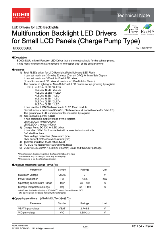
●Description BD6085GUL is Multi-Function LED Driver that is the most suitable for the cellular phone. It has many functions that are needed to "the upper side" of the cellular phone.

●Features 1) Total 7LEDs driver for LCD Backlight (Main/Sub) and LED Flash It can set maximum 30m A by 32 steps (Current DAC) for Main/Sub Display It can set maximum 360m A for Flash LED driver (It has 3 channels LED driver at maximum 120m A/ch for Flash.) The number of lighting for Main/Sub/Flash LED can be set up grouping by register. Ex. ) 4LEDs / 0LED / 3LEDs 4LEDs / 1LED / 2LEDs 4LEDs / 2LEDs / 1LED 4LEDs / 1LED / 1LED 5LEDs / 1LED / 1LED 5LEDs / 0LED / 2LEDs 6LEDs / 0LED / 1LED It can use the 1LED Flash module to 3LED Flash module. Normal mode = maximum 30m A/ch, Flash mode = x4 normal mode (for 3ch LED). The grouping of LED is independently controlled by register. 2) 4ch Series Regulator (LDO) It has selectable output voltage by the register. LDO1,LDO2 : Iomax=200m A LDO3,LDO4 : Iomax=150m A 3) Charge Pump DC/DC for LED driver It has x1/x1.33/x1.5/x2 mode that will be selected automatically. Soft start functions Over voltage protection (Auto-return type) Over current protection (Auto-return type) 4) Thermal shutdown (Auto-return type) 5) I2C BUS FS mode(max 400k Hz)Write/Read 6) VCSP50L3(3.30mm×3.30mm, 0.55mm) Small and thin CSP package

*This chip is not designed to protect itself against radioactive rays. *This material may be changed on its way to designing. *This material is not the official specification.

●Absolute Maximum Ratings (Ta=25 ℃)

Parameter Symbol Ratings Unit

Maximum voltage VMAX 7 V Power Dissipation Pd 1325 m W Operating Temperature Range Topr -35 ~ +85 ℃ Storage Temperature Range Tstg -55 ~ +150 ℃ note)Power dissipation deleting is 10.6m W/ ℃, when it’s used in over 25 ℃. (It’s deleting is on the board that is ROHM’s standard)

●Operating conditions (VBAT≥VIO, Ta=-35~85 ℃)

Parameter Symbol Ratings Unit

VBAT input voltage VBAT 2.7~5.5 V VIO pin voltage VIO 1.65~3.3 V

www.rohm.com 2011.04 - Rev.A

© 2011 ROHM Co., Ltd. All rights reserved.

Page Summary Contents For ROHM BD6085GUL Data Sheet

Page 1 LED Drivers for LCD Backlights Multifunction Backlight LED Drivers for Small LCD Panels (Charge Pump Type) BD6085GUL No.11040EAT28 ●Description BD6085GUL is Multi-Function LED Driver that is the most ...
Page 2 BD6085GUL Technical Note ●Electrical Characteristics (Unless otherwise specified, Ta=25°C, VBAT=3.6V, VIO=1.8V) Limits Parameter Symbol Unit Condition Min. Typ. Max. 【Circuit Current】 VBAT Circuit cur...
Page 3 BD6085GUL Technical Note ●Electrical Characteristics (Unless otherwise specified, Ta=25°C, VBAT=3.6V, VIO=1.8V) Limits Parameter Symbol Unit Condition Min. Typ. Max. 【Regulator (LDO1)】 1.164 1.20 1.23...
Page 4 BD6085GUL Technical Note ●Electrical Characteristics (Unless otherwise specified, Ta=25°C, VBAT=3.6V, VIO=1.8V) Limits Parameter Symbol Unit Condition Min. Typ. Max. 【Regulator (LDO3)】 1.164 1.20 1.23...
Page 5 BD6085GUL Technical Note ●Block Diagram / Application Circuit example VBATCP VBAT1 Charge Pump VBAT2 VBATLDO1 x1 / x1.33 / x1.5 / x2 (6.3V) VBATLDO2 LED1~4 Charge Pump OVP Mode Control LED terminal vo...
Page 6 BD6085GUL Technical Note VBATCP VBAT1 Charge Pump VBAT2 VBATLDO1 x1 / x1.33 / x1.5 / x2 (6.3V) VBATLDO2 LED1~6 Charge Pump OVP Mode Control LED terminal voltage feedback Back Light Main only or (O pe ...
Page 7 BD6085GUL Technical Note ●Pin Arrangement [Bottom View] F T4 VBATLDO2 VBAT1 AGND VBATLDO1 T3 E LDO2O LDO4O VBAT2 LDO3O LDO1O VIO D LED6 LED7 RESETB SCL SDA C1N C LED5 FLGND CPGND C2N C1P B LED4 WGND L...
Page 8 BD6085GUL Technical Note ●Package VCSP50L3 SIZE : 3.30mm×3.30mm A ball pitch : 0.5mm Height : 0.55mm max BD6085 Lot No. www.rohm.com 2011.04 - Rev.A © 2011 ROHM Co., Ltd. All rights reserved.
Page 9 BD6085GUL Technical Note ●Pin Functions ESD Diode Ball Equivalent No Pin Name I/O For For Functions No. Circuit Power Ground 1 B6 VBATCP - - GND Power supply for charge pump A 2 F3 VBAT1 - - GND Power...
Page 10 BD6085GUL Technical Note ●Equivalent Circuit VBATCA VBATB VBATD VBAT F G VIOVBAT H VIO VBAT I VIOVBAT J VBATVBAT L VIOVIOK VBAT VBAT M VBATN VBATO VBAT VBATP VBAT VBAT Q VBATVBAT R VBATVBATS VIO VBATT...
Page 11 BD6085GUL Technical Note ●I2C BUS format The writing/reading operation is based on the I2C slave standard. ・Slave address A7 A6 A5 A4 A3 A2 A1 R/W 1 1 1 0 1 1 0 1/0 ・Bit Transfer SCL transfers 1-bit d...
Page 12 BD6085GUL Technical Note ・Writing protocol A register address is transferred by the next 1 byte that transferred the slave address and the write-in command. The 3rd byte writes data in the internal re...
Page 13 BD6085GUL Technical Note ●Timing diagram t BUF t SU;DAT t HD;STA t LOW t SU;STO t SU;STA t HD;STA t HD;DAT S Sr P S t HIGH ●Electrical Characteristics(Unless otherwise specified, Ta=25 ℃, VBAT=3.6V, V...
Page 14 BD6085GUL Technical Note ●Register List Register data Address Function Software Reset 00h - GRPSET2 GRPSET1 GRPSET0 - - - SFTRST LED Lighting group Setting 01h - LDO4EN LDO3EN LDO2EN LDO1EN FLLEDEN SL...
Page 15 BD6085GUL Technical Note Address 01h < Enable Control > Address R/W Bit7 Bit6 Bit5 Bit4 Bit3 Bit2 Bit1 Bit0 01h R/W - LDO4EN LDO3EN LDO2EN LDO1EN FLLEDEN SLEDEN MLEDEN Initial Value Bit7 : (Not ...
Page 16 BD6085GUL Technical Note Address 02h < Main LED Current Setting > Address R/W Bit7 Bit6 Bit5 Bit4 Bit3 Bit2 Bit1 Bit0 02h R/W - - - IMLED4 IMLED3 IMLED2 IMLED1 IMLED0 Initial Value Bit[7:5] : (N...
Page 17 BD6085GUL Technical Note Address 03h < Sub LED Current Setting > Address R/W Bit7 Bit6 Bit5 Bit4 Bit3 Bit2 Bit1 Bit0 03h R/W - - - ISLED4 ISLED3 ISLED2 ISLED1 ISLED0 Initial Value Bit[7:5] : (No...
Page 18 BD6085GUL Technical Note Address 04h < Flash LED Current Setting, Flash mode Setting > Address R/W Bit7 Bit6 Bit5 Bit4 Bit3 Bit2 Bit1 Bit0 04h R/W - - FLASHEN IFLLED4 IFLLED3 IFLLED2 IFLLED1 IFL...
Page 19 BD6085GUL Technical Note Address 05h < LDO1 Vout Control, LDO2 Vout Control > Address R/W Bit7 Bit6 Bit5 Bit4 Bit3 Bit2 Bit1 Bit0 05h R/W LDO2VSEL3 LDO2VSEL2 LDO2VSEL1 LDO2VSEL0 LDO1VSEL3 LDO1VS...
Page 20 BD6085GUL Technical Note Address 06h < LDO3 Vout Control, LDO4 Vout Control > Address R/W Bit7 Bit6 Bit5 Bit4 Bit3 Bit2 Bit1 Bit0 06h R/W LDO4VSEL3 LDO4VSEL2 LDO4VSEL1 LDO4VSEL0 LDO3VSEL3 LDO3VS...
Page 21 BD6085GUL Technical Note ●Explanation for operate 1. Reset There are two kinds of reset, software reset and hardware reset. (1) Software reset ・All the registers are initialized more than making a reg...
Page 22 BD6085GUL Technical Note Charge Pump Mode transition The transition of boost multiple transits automatically by Vf of LED and the battery voltage. STANDBY ALL off Any LED on ○1 Ta<TTSD VBAT>2.3V...
Page 23 BD6085GUL Technical Note 4. LED Driver LED current value setting (for Main/Sub) Internal circuit fixes maximum current value of LED. LED current is maximum 30m A/ch. LED current value setting (for Fla...
Page 24 BD6085GUL Technical Note 5. I/O When the RESETB pin is Low, the input buffers (SDA and SCL) are disable for the Low consumption power. RESETB=L, Output “H” SCL (SDA) EN Level LOGIC Shift RESETB 6. Abo...
Page 25 BD6085GUL Technical Note ●PCB pattern of the Power dissipation measuring board 1st layer(component) 2nd layer 3rd layer 4th layer 5th layer 6th layer 7th layer 8th layer(solder) www.rohm.com 2011.04 -...
Page 26 BD6085GUL Technical Note ●Cautions on use (1) Absolute Maximum Ratings An excess in the absolute maximum ratings, such as supply voltage, temperature range of operating conditions, etc., can break dow...
Page 27 BD6085GUL Technical Note ●Power dissipation (On the ROHM’s standard board) is si pa ti Ta(℃) Information of the ROHM’s standard board Material : glass-epoxy Size : Refer to after page. www.rohm.com 20...
Page 28 BD6085GUL Technical Note ●Ordering part number Part No. Part No. Package Packaging and forming specification GUL : VCSP50L3 E2: Embossed tape and reel VCSP50L3(BD6085GUL) <Tape and Reel information...
Page 29 Notice No copying or reproduction of this document, in part or in whole, is permitted without the consent of ROHM Co.,Ltd. The content specified herein is subject to change for improvement without not...

Manual Details

Brand ROHM
Pages 29
File Size 470.74 KB
Published June 02, 2026
80 views

Enter the captcha to get the download link:

captcha

Frequently Asked Questions

How can the LED lighting be adjusted across Main, Sub, and Flash segments?

The number of LEDs for Main/Sub/Flash can be grouped and independently controlled by registers (e.g., 4LEDs / 1LED / 2LEDs).

What is the maximum continuous flash current available?

The system supports setting a maximum of 360mA for the Flash LED driver, utilizing up to three channels at a maximum of 120mA/channel.

What are the acceptable input voltage ranges needed for operation?

The recommended operating conditions require an input voltage (VBAT) between 2.7V and 5.5V, while the VIO pin should be maintained between 1.65V and 3.3V.

Does this driver have protection against common electrical failures?

Yes, it features over voltage, over current, and thermal shutdown protections, all of which are auto-return types.