ROHM DTB713ZE Data Sheet
Summary
These low saturation voltage digital transistors are perfect for designing robust inverter, interface, and driver circuits. Featuring built-in bias resistors and superior isolation, the DTB713 series significantly simplifies circuit setup by eliminating the need for external input components. This manual details electrical characteristics, maximizing efficiency and ease of use for electronics engineers tackling demanding power management applications.
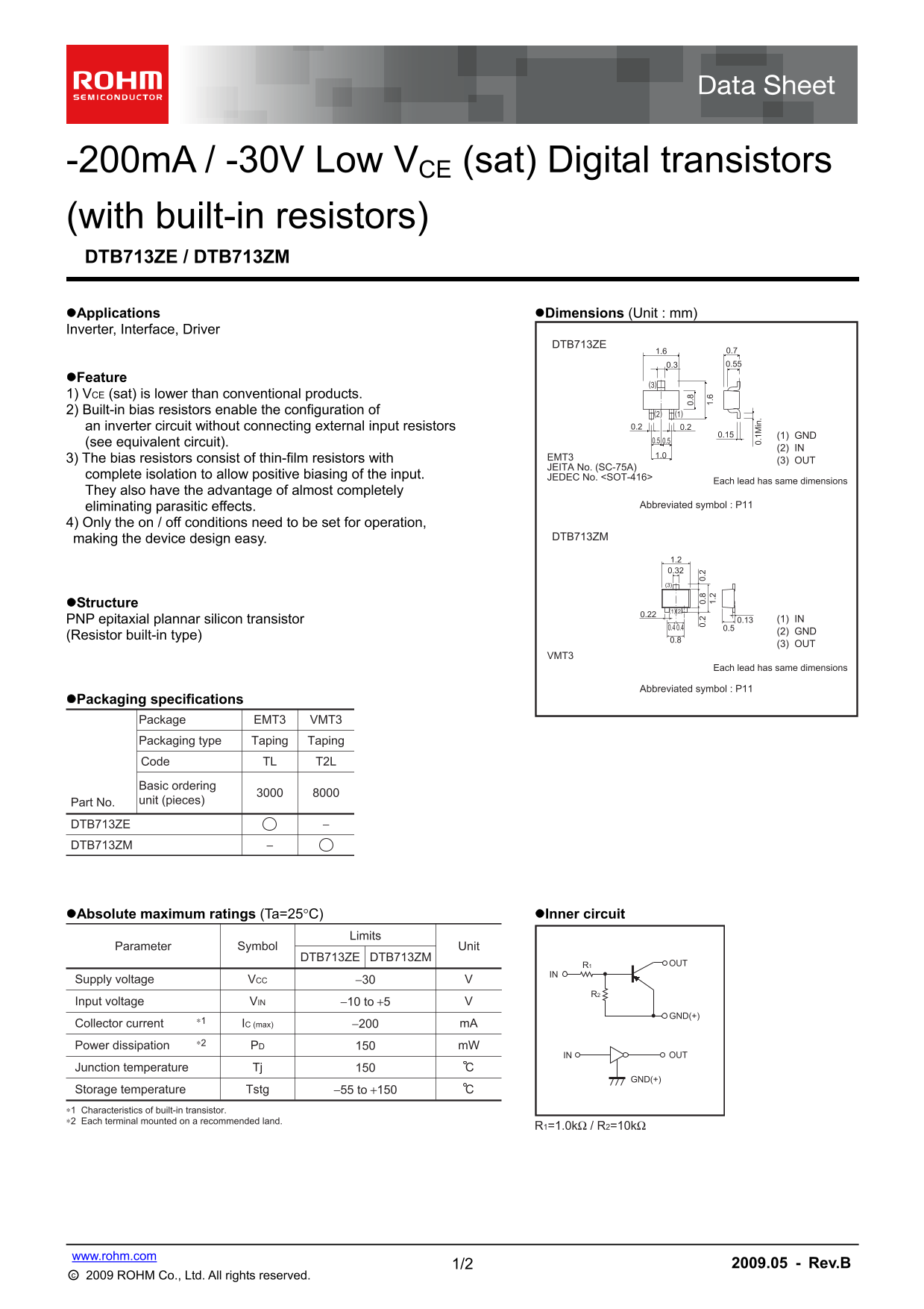
Page 1 Text Content
-200m A / -30V Low VCE (sat) Digital transistors (with built-in resistors) DTB713ZE / DTB713ZM Applications Dimensions (Unit : mm) Inverter, Interface, Driver
DTB713ZE
Feature
1) VCE (sat) is lower than conventional products. 2) Built-in bias resistors enable the configuration of (2) (1)
an inverter circuit without connecting external input resistors 0.2 0.2
0.15 (1) GND
(see equivalent circuit). 0.50.5
(2) IN
EMT3 1.0
3) The bias resistors consist of thin-film resistors with (3) OUT
JEITA No. (SC-75A)
complete isolation to allow positive biasing of the input. JEDEC No. <SOT-416>
Each lead has same dimensions
They also have the advantage of almost completely
eliminating parasitic effects. Abbreviated symbol : P11
4) Only the on / off conditions need to be set for operation,
making the device design easy. DTB713ZM
Structure
PNP epitaxial plannar silicon transistor 0.13 (1) IN
(2) GND
(Resistor built-in type)
(3) OUT
Each lead has same dimensions
Abbreviated symbol : P11 0.
Packaging specifications 0. 0. 0.
Package EMT3 VMT3 Packaging type Taping Taping
0. 1M in
Code TL T2L
Basic ordering Part No. unit (pieces)
DTB713ZE DTB713ZM
Absolute maximum ratings (Ta=25°C) Inner circuit
Limits
Parameter Symbol Unit
DTB713ZE DTB713ZM
R1 OUT
Supply voltage VCC −30
Input voltage VIN −10 to +5
GND(+)
Collector current IC (max) −200 m A
Power dissipation PD m W
IN OUT
Junction temperature Tj
GND(+)
Storage temperature Tstg −55 to +150
∗1 Characteristics of built-in transistor. ∗2 Each terminal mounted on a recommended land.
1/2 www.rohm.com 2009.05 - Rev.B
○c 2009 ROHM Co., Ltd. All rights reserved.
Page Summary Contents For ROHM DTB713ZE Data Sheet
Manual Details
| Brand | ROHM |
|---|---|
| Pages | 3 |
| File Size | 179.15 KB |
| Published | July 16, 2026 |
Enter the captcha to get the download link:

Frequently Asked Questions
How can I configure an inverter circuit?
You can use the built-in bias resistors, which enable configuration without connecting external input resistors.
What are the maximum operating ratings for this transistor?
The max collector current is -200 mA, and the power dissipation (Pd) is 150 mW at 25°C.
What voltage range should I use for the input signal (Vin)?
The recommended range for the Input Voltage (VIN) is from -10 to +5 V, given a VCC of -30V.