ROHM DTB513ZE DTB513ZM User Guide and Manual
Summary
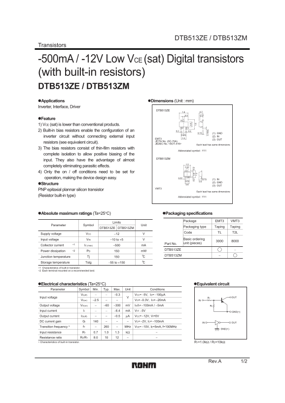
These advanced digital transistors are engineered for high-efficiency interfaces and driving applications in low-voltage circuits, featuring built-in resistors for simplified circuit design. Designed with low VCE(sat) performance, they simplify the configuration of inverter circuits by eliminating the need for external bias components. This comprehensive manual provides engineers with complete electrical ratings, application guidelines, and functional characteristics needed to reliably integrate these planar silicon transistors into complex interface and driver systems.
Page 1 Text Content
DTB513ZE DTB513ZM
Transistors
-500m A / -12V Low VCE (sat) Digital transistors (with built-in resistors) DTB513ZE / DTB513ZM Applications Dimensions (Unit : mm) Inverter, Interface, Driver
DTB513ZE
Feature
1) VCE (sat) is lower than conventional products.
2) Built-in bias resistors enable the configuration of an 0.2 0.2
0.15 (1) GND
inverter circuit without connecting external input (2) IN
EMT3 1.0
(3) OUT
JEITA No. (SC-75A)
resistors (see equivalent circuit).
JEDEC No. <SOT-416> Each lead has same dimensions
3) The bias resistors consist of thin-film resistors with
Abbreviated symbol : Y11
complete isolation to allow positive biasing of the
DTB513ZM
input. They also have the advantage of almost
completely eliminating parasitic effects. 0.32
4) Only the on / off conditions need to be set for
operation, making the device design easy. 0.22
0.13 (1) IN
(2) GND
Structure 0.8
(3) OUT
PNP epitaxial plannar silicon transistor 0.
Each lead has same dimensions
(Resistor built-in type) 1. 1.
Abbreviated symbol : Y11
0. 1M in
Absolute maximum ratings (Ta=25 C) Packaging specifications
Package EMT3 VMT3
Limits
Parameter Symbol Unit
Packaging type Taping Taping
DTB513ZE DTB513ZM
Code TL T2L
Supply voltage VCC −12
Input voltage VIN −10 to +5 Basic ordering Part No. unit (pieces)
Collector current ∗1 IC (max) m A
∗2 DTB513ZE
Power dissipation PD m W
DTB513ZM
Junction temperature Tj Storage temperature Tstg −55 to +150
∗1 Characteristics of built-in transistor. ∗2 Each terminal mounted on a recommended land.
Electrical characteristics (Ta=25 C) Equivalent circuit Parameter Symbol Min. Typ. Max. Unit Conditions
VI(off) −0.3 VCC= −5V, IO= −100μA
Input voltage R1 OUT
VI(on) −2.5 VO= −0.3V, IO= −20m A IN Output voltage VO(on) −60 −300 m V IO/II= −100m A / −5m A R2
Input current II −6.4 m A VI= −5V GND(+) Output current IO(off) −0.5 μA VCC= −12V, VI=0V
DC current gain GI VO= −2V, IO= −100m A
IN OUT
Transition frequency f T MHz VCE= −10V, IE=5m A, f=100MHz
GND(+)
Input resistance R1 0.7 1.0 1.3 kΩ Resistance ratio R2/R1 8.0
∗ Characteristics of built-in transistor. R1=1.0kΩ / R2=10kΩ
Rev.A 1/2
Page Summary Contents For ROHM DTB513ZE DTB513ZM User Guide and Manual
Manual Details
| Brand | ROHM |
|---|---|
| Pages | 3 |
| File Size | 69.86 KB |
| Published | June 18, 2026 |
Enter the captcha to get the download link:

Frequently Asked Questions
How do the built-in bias resistors help simplify circuit design?
They enable an inverter configuration without connecting external inputs, while also almost completely eliminating parasitic effects.
What is the maximum collector current and power dissipation rating?
The maximum collector current (IC) is -500 mA, and the power dissipation (PD) is rated at 150 mW.
Can I use this transistor in life-critical equipment like medical instruments?
No. For high reliability devices that could endanger human life, you must consult a sales representative first.
What is the specified operating range for the input voltage (VIN)?
The Input Voltage (VIN) can operate within the range of -10 V to +5 V.