# A B C D E F G H I J K L M N O P Q R S T U V W X Y Z

ROHM BU9910KV Data Sheet

Summary

This integrated LCD driver, BU9910KV, is designed for complex PC and multimedia display systems. It manages up to 44 LCD cells using a flexible I²C bus interface and provides 20 direct drive inputs for simple system configuration. The accompanying manual details comprehensive technical specifications, including pin mappings, various operating modes, power supply requirements (3.3V to 5.5V), and detailed timing diagrams necessary for integration into custom electro-optical applications.
📄 Preview PAGE OF 15

Page 1 Text Content

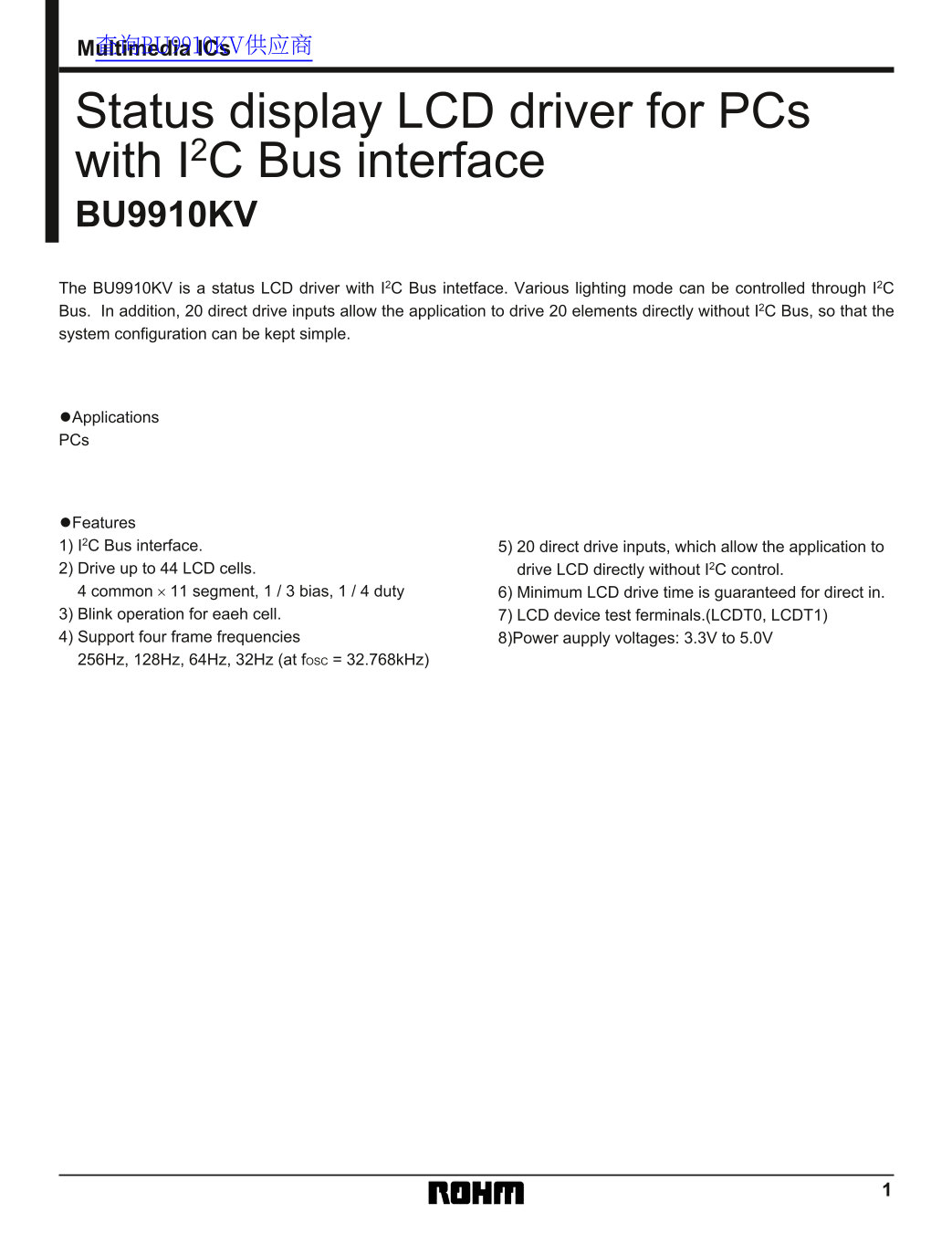
Multimedia ICs 查询BU9910KV供应商

Status display LCD driver for PCs with I2C Bus interface BU9910KV The BU9910KV is a status LCD driver with I2C Bus intetface. Various lighting mode can be controlled through I2C Bus. In addition, 20 direct drive inputs allow the application to drive 20 elements directly without I2C Bus, so that the system configuration can be kept simple.

•Applications PCs

•Features 1) I2C Bus interface. 5) 20 direct drive inputs, which allow the application to 2) Drive up to 44 LCD cells. drive LCD directly without I2C control. 4 common × 11 segment, 1 / 3 bias, 1 / 4 duty 6) Minimum LCD drive time is guaranteed for direct in. 3) Blink operation for eaeh cell. 7) LCD device test ferminals.(LCDT0, LCDT1) 4) Support four frame frequencies 8)Power aupply voltages: 3.3V to 5.0V

256Hz, 128Hz, 64Hz, 32Hz (at f OSC = 32.768k Hz)

Page Summary Contents For ROHM BU9910KV Data Sheet

Page 1 Multimedia ICs 查询BU9910KV供应商 Status display LCD driver for PCs with I2C Bus interface BU9910KV The BU9910KV is a status LCD driver with I2C Bus intetface. Various lighting mode can be controlled throu...
Page 2 Multimedia ICs BU9910KV •Block diagram L3 IN L2 IN 37SEG10 DIN7 L1 IN Date Latch Logic SEG9 DIN6 SEG8 DIN5 IN Control Logic SEG7 DIN4 SEG6 DIN3 I2CBus IN Segment Interface SEG5 Driver DIN2 LK IN SEG4 ...
Page 3 Multimedia ICs BU9910KV •Pin descriptions Pin No. Pin name Function VL3 Input for LCD driver VL2 Input for LCD driver (2 / 3) ∗VL3 VL1 Input for LCD driver (1 / 3) ∗VL3 GND Ground COM3 LCD common driv...
Page 4 Multimedia ICs BU9910KV Pin No. Pin name Function SEG10 LCD segment driver output 10 SEG9 LCD segment driver output 9 SEG8 LCD segment driver output 8 SEG7 LCD segment driver output 7 SEG6 LCD segment...
Page 5 Multimedia ICs BU9910KV •Input / output circuits Pin No. Pin name Equivalent circuit Pin description SDA I2C Bus serial data input / output. SCL I2C Bus serial clock Input. Clock Input for LCD display...
Page 6 Multimedia ICs BU9910KV Pin No. Pin name Equivalent circuit Pin description COM0 ~ 5 ~ 8 LCD common drive output. SEG0 ~ 37 ~ 47 LCD segment drive output. SEG10 Input of LCD drive voltage setting. Sup...
Page 7 Multimedia ICs BU9910KV Pin No. Pin name Equivalent circuit Pin description Hold time setting terminal of the direct HT0 ~ 15 ~ 16 drive input. There are four hold times to drive the cell. 30kΩ: VDD =...
Page 8 Multimedia ICs BU9910KV •Application example VDD COM0VDD SEG1 Segment VL1 LCD Power on Reset #RES CLK SEG10 fosc = 32.768k Hz I2C Bus Controller Set direct in HT0 HT1 Direct In hold time (HDD.FDD.etc)...
Page 9 Multimedia ICs BU9910KV •Circuit operation (1) Description of the I2C Bus interface 1) Slave address MSB LSB 2) Conformance to I2C Bus standards Parameter Symbol Min. Max. Unit SCL clock frequency f S...
Page 10 Multimedia ICs BU9910KV (2) Data structure 1) Wrote Mode Address ACommand Reg. Byte Write Data Byte Auto Increment 2) Read Mode 1. Command register set Address ACommand Reg. Byte Sr Address AR PRead D...
Page 11 Multimedia ICs BU9910KV D3 to D0: Pointer register The Pointer register appoints a base address, which acceses the LCD display memory in read or write mode. In the write mode, a byte data that follows...
Page 12 Multimedia ICs BU9910KV Blink control memory: SEG vs. COM(COM No. / SEG No.) Base Address bit7 bit6 bit5 bit4 bit3 bit2 bit1 bit0 3) Direct drive input description Direct input pin vs.SEG / COM SEG6 S...
Page 13 Multimedia ICs BU9910KV (4) Output waveforms (1 / 2) To = 1 / fo • COM 0 Drive Output VL2 VL1 VSS • COM 1 Drive Output VL2 VL1 VSS • COM 2 Drive Output VL2 VL1 VSS • COM 3 Drive Output VL2 VL1 VSS VL3...
Page 14 Multimedia ICs BU9910KV (5) Output waveforms (2 / 2) To = 1 / fo • COM 0 Drive Output VL2 VL1 VSS • COM 1 Drive Output VL2 VL1 VSS • COM 2 Drive Output VL2 VL1 VSS • COM 3 Drive Output VL2 VL1 VSS VL3...
Page 15 Multimedia ICs BU9910KV •External dimensions (Units: mm) VQFP48

Manual Details

Brand ROHM
Pages 15
File Size 90.83 KB
Published July 22, 2026
0 views

Enter the captcha to get the download link:

captcha

Frequently Asked Questions

What is the operating voltage range for this IC?

The recommended supply voltage (VDD) is from 3.0V to 5.5V.

How many direct drive inputs are available?

There are 20 direct drive inputs, allowing direct driving without using the I²C Bus.

What specific clock frequency is designed for this IC?

The CLK input expects a clock frequency of 32.768kHz.

Which pins handle the LCD segment driver outputs and common drivers?

The SEG0-SEG10 pins handle segment outputs, while COM0-COM3 pins manage the common drive outputs.