ROHM BU9718KV Picture Cell Driver for STN Owners Manual
Summary
The BU9718KV is a specialized driver IC designed for character-type STN liquid crystal displays, enabling the operation of up to 96 segments in low-voltage applications. Ideal for engineers designing compact electronic instruments such as portable terminals (POS, PDA) or handheld devices. This comprehensive manual provides detailed technical specifications, including electrical characteristics, AC timing diagrams, pin assignments, and multiple application examples, ensuring reliable integration into your next product build.
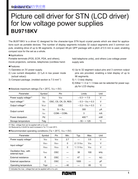
Page 1 Text Content
Standard ICs 查询BU9718KV供应商
Picture cell driver for STN (LCD driver) for low voltage power supplies BU9718KV The BU9718KV is a driver IC designed for the character-type STN liquid crystal panels which are ideal for applica- tions such as portable devices. The number of display segments includes 32 output segments and 3 common out- puts, enabling drive of up to 96 segments. A compact 48-pin QFP package with a pitch of 0.5 mm is used, enabling compact size for the set as a whole. •Applications Portable terminals (POS, ECR, PDA, and others), held telephone units), and others Low-voltage power movie projectors, cameras, telephones (cordless hand- supply sets •Features
1) Operates on 3V power supply. 4) Up to 32 segment output pins and 3 common output 2) Low current dissipation. (0.1µA in low power mode pins are provided, enabling a total display of up to (actual value)) 96 segments. 3) Compact package. (molded section is 7.0 mmu) 5) 1 / 3 duty display. 6) Either 1 / 2 or 1 / 3 bias can be selected for power sup- ply for LCD display.
•Absolute maximum ratings (Ta = 25°C, VSS = 0V)
Parameter Symbol Pin Limits Unit
Power supply voltage∗1 VDD VDD – 0.3 ~ + 7.0
Input voltage∗1 VIN OSC, CS, CK, DI, RES – 0.3 ~ VDD + 0.3
Output voltage∗1 VOUT OSC – 0.3 ~ VDD + 0.3
ISO S1 ~ S32 µA
Output current
ICO 3COM1 ~ COM3 m A
Power dissipation Pd 400 ∗2 — m W
Storage temperature Tstg – 55 ~ + 125— °C
∗1 Max. voltage that can be applied with a VSS pin ∗2 Reduced by 4.0m W for each increase in Ta 1°C over 25°C.
•Recommended operating conditions (Ta = 25°C, VSS = 0V)
Parameter Symbol Pin Min. Typ. Max. Unit
Power supply voltage∗ VDD VDD 2.7 3.5
VDD1 2 / 3 VDD VDD VVDD1
Input voltage∗
VDD2 1 / 3 VDD VDD VVDD2
Oscillation freq., with
f OSC k Hz OSC
external input External resistance kΩOSC
External capacitance p FOSC
Operating temperature Topr – 40 °C— ∗ Indicates the max. voltage that can be applied with a VSS pin.
Page Summary Contents For ROHM BU9718KV Picture Cell Driver for STN Owners Manual
Manual Details
| Brand | ROHM |
|---|---|
| Pages | 10 |
| File Size | 78.66 KB |
| Published | May 31, 2026 |
Enter the captcha to get the download link:

Frequently Asked Questions
What is the required operating voltage range for the BU9718KV IC?
The minimum power supply voltage (VDD) must be between 2.7 V and 3.5 V.
How do I reset the device when external reset terminals are used during startup?
Set the external reset terminal (RST) to 'L' for at least 1 ms while ensuring VDD is 2.7V or more.
What is the maximum segment capacity and output structure of this driver IC?
It enables drive of up to 96 segments, utilizing 32 output segments and 3 common outputs.
Are specific external component values needed when integrating this device?
Yes, the resistance and capacitance values should be set to match the LCD panel being used.
How can I configure the power supply bias for the liquid crystal display?
You can select either a 1/2 bias or a 1/3 bias using the dedicated internal standard voltage pins (VDD1/VDD2).