ROHM BU9006GUZ Data Sheet
Summary
Optimize your power management solutions with this high-efficiency Synchronous Rectifier Step-down DC-DC Converter. Designed for reliability in general electronic applications like audio, office automation, and communication devices, it provides precise voltage regulation across a wide input range (2.5V–4.5V). This technical summary covers comprehensive operational data, detailed electrical characteristics, power dissipation ratings, and crucial design guidelines needed by electrical engineers and embedded systems developers to ensure optimal product performance and integration.
Page 1 Text Content
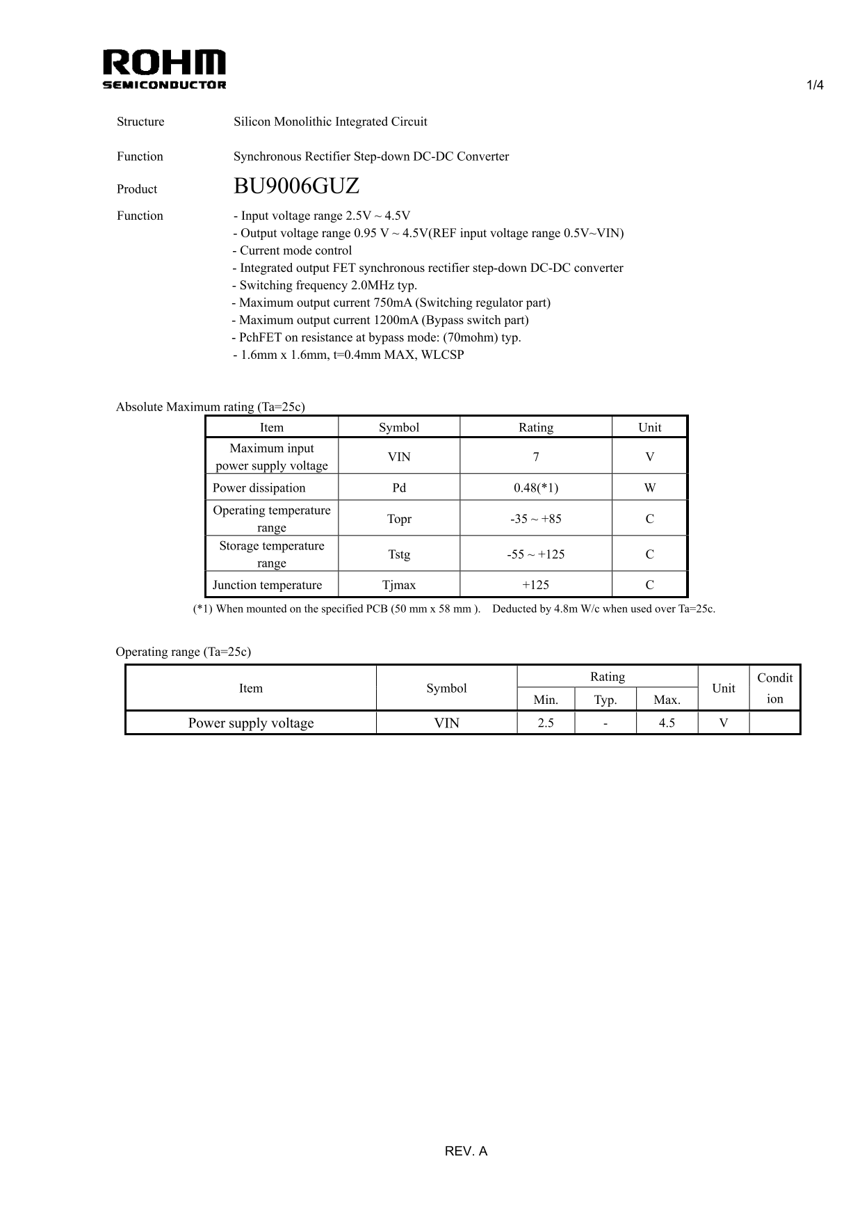
Structure Silicon Monolithic Integrated Circuit
Function Synchronous Rectifier Step-down DC-DC Converter
Product BU9006GUZ
Function - Input voltage range 2.5V ~ 4.5V - Output voltage range 0.95 V ~ 4.5V(REF input voltage range 0.5V~VIN)
- Current mode control - Integrated output FET synchronous rectifier step-down DC-DC converter - Switching frequency 2.0MHz typ. - Maximum output current 750m A (Switching regulator part) - Maximum output current 1200m A (Bypass switch part) - Pch FET on resistance at bypass mode: (70mohm) typ. - 1.6mm x 1.6mm, t=0.4mm MAX, WLCSP
Absolute Maximum rating (Ta=25c)
Item Symbol Rating Unit Maximum input
VIN 7 V
power supply voltage Power dissipation Pd 0.48(*1) W Operating temperature
Topr -35 ~ +85 C
range Storage temperature
Tstg -55 ~ +125 C
range Junction temperature Tjmax +125 C
(*1) When mounted on the specified PCB (50 mm x 58 mm ). Deducted by 4.8m W/c when used over Ta=25c.
Operating range (Ta=25c)
Rating Condit
Item Symbol Unit
ion Min. Typ. Max.
Power supply voltage VIN 2.5 - 4.5 V
REV. A
Page Summary Contents For ROHM BU9006GUZ Data Sheet
Manual Details
| Brand | ROHM |
|---|---|
| Pages | 5 |
| File Size | 114.86 KB |
| Published | July 15, 2026 |
Enter the captcha to get the download link:

Frequently Asked Questions
What is the maximum input voltage (VIN) and power dissipation?
The maximum input voltage is 7V, with a power dissipation of up to 0.48W on specified PCBs.
How should I manage thermal design for this component?
Use a thermal design that allows sufficient margin considering the power dissipation (Pd) in actual operating conditions.
Is there a built-in circuit to prevent overheating?
Yes, this model IC has a built-in Thermal shutdown Circuit (TSD Circuit), designed only to cut off thermal runaway.
What must I keep in mind regarding grounding and electrical connections?
The potential of the GND pin must be the minimum potential; also use caution to minimize mutual impedance.