# A B C D E F G H I J K L M N O P Q R S T U V W X Y Z

ROHM BU1852GUW Data Sheet

Summary

The Keyencoder IC BU1852GUW is a high-functionality semiconductor designed to monitor complex keyboard matrices, supporting up to 96 keys in a Qwerty format. It significantly reduces CPU load by encoding only the change status of pressed or released keys, rather than storing all key states. This device offers advanced features like N-key Rollover, ghost key rejection, and built-in Power on Reset. Ideal for electronic device manufacturers (such as audio/visual, office automation, or amusement equipment) who require robust, low-power input monitoring and flexible GPIO selectability while needing ultra-low standby current consumption.
📄 Preview PAGE OF 25

Page 1 Text Content

GPIO ICs

Keyencoder IC

BU1852GUW No.11098EAT04

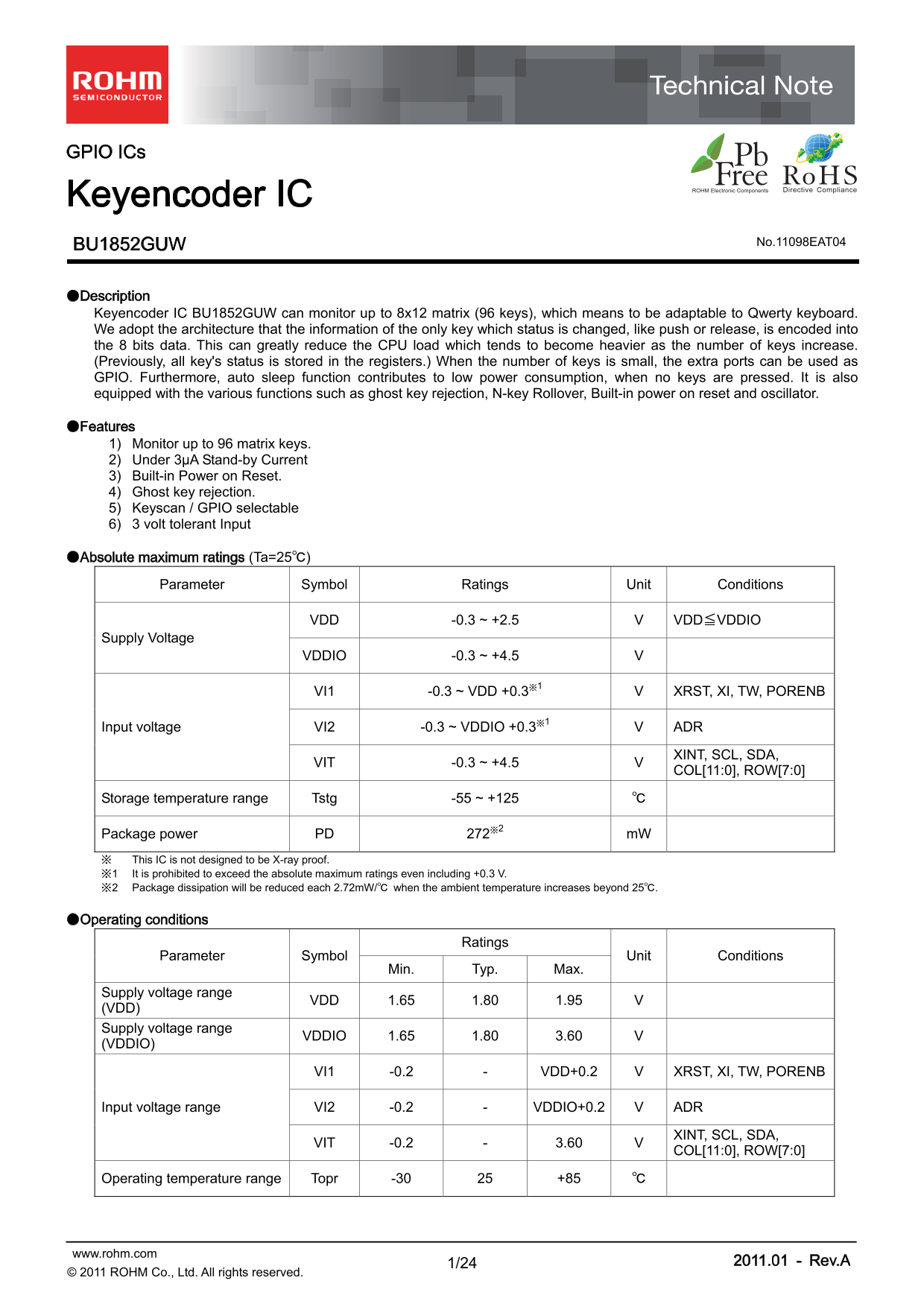
●Description Keyencoder IC BU1852GUW can monitor up to 8x12 matrix (96 keys), which means to be adaptable to Qwerty keyboard. We adopt the architecture that the information of the only key which status is changed, like push or release, is encoded into the 8 bits data. This can greatly reduce the CPU load which tends to become heavier as the number of keys increase. (Previously, all key's status is stored in the registers.) When the number of keys is small, the extra ports can be used as GPIO. Furthermore, auto sleep function contributes to low power consumption, when no keys are pressed. It is also equipped with the various functions such as ghost key rejection, N-key Rollover, Built-in power on reset and oscillator.

●Features 1) Monitor up to 96 matrix keys. 2) Under 3µA Stand-by Current 3) Built-in Power on Reset. 4) Ghost key rejection. 5) Keyscan / GPIO selectable 6) 3 volt tolerant Input

●Absolute maximum ratings (Ta=25℃)

Parameter Symbol Ratings Unit Conditions

VDD -0.3 ~ +2.5 V VDD≦VDDIO

Supply Voltage

VDDIO -0.3 ~ +4.5 V

VI1 -0.3 ~ VDD +0.3※1 V XRST, XI, TW, PORENB

Input voltage VI2 -0.3 ~ VDDIO +0.3※1 V ADR

VIT -0.3 ~ +4.5 V XINT, SCL, SDA,

COL[11:0], ROW[7:0]

Storage temperature range Tstg -55 ~ +125 ℃

Package power PD 272※2 m W ※ This IC is not designed to be X-ray proof. ※1 It is prohibited to exceed the absolute maximum ratings even including +0.3 V. ※2 Package dissipation will be reduced each 2.72m W/℃ when the ambient temperature increases beyond 25℃.

●Operating conditions

Ratings

Parameter Symbol Unit Conditions

Min. Typ. Max.

Supply voltage range (VDD) VDD 1.65 1.80 1.95 V Supply voltage range

VDDIO 1.65 1.80 3.60 V

(VDDIO)

VI1 -0.2 - VDD+0.2 V XRST, XI, TW, PORENB

Input voltage range VI2 -0.2 - VDDIO+0.2 V ADR

XINT, SCL, SDA,

VIT -0.2 - 3.60 V

COL[11:0], ROW[7:0]

Operating temperature range Topr -30 25 +85 ℃

www.rohm.com 2011.01 - Rev.A 1/24 © 2011 ROHM Co., Ltd. All rights reserved.

Page Summary Contents For ROHM BU1852GUW Data Sheet

Page 1 GPIO ICs Keyencoder IC BU1852GUW No.11098EAT04 ●Description Keyencoder IC BU1852GUW can monitor up to 8x12 matrix (96 keys), which means to be adaptable to Qwerty keyboard. We adopt the architecture t...
Page 2 BU1852GUW Technical Note ●Electrical characteristics 1. DC characteristics (VDD=1.8V, VDDIO=1.8V, Ta=25℃) Limits Parameter Symbol Unit Conditions Min. Typ. Max. Input H Voltage1 VIH1 0.8x VDD - 3.6 V ...
Page 3 BU1852GUW Technical Note 3. I2C AC Characteristics (Repeated) BIT7 BIT6 Ack STOPCondition START t SU;STA 1/f SCLK t HIGH t LOW t SU;STO t SU;DAT t BUF t HD;STA t HD;DAT Fig.1 I2C AC timing VDD=1.8V, V...
Page 4 BU1852GUW Technical Note 4. GPIO AC Characteristics BIT 0BIT 1 NAState GPIO[7:0](Output) GPIO[7:0](Input) t IV t IR Fig.2 GPIO AC timing VDD=1.8V, VDDIO=1.8V, Topr=25℃, TW=VSS Limits Parameter Symbol ...
Page 5 BU1852GUW Technical Note 5. Startup sequence t VDD t VDD VDD t VDD VDDIO t RWAIT t RWAIT XRST t VDD t I2CWAIT t I2CWAIT Fig.3 Start Sequence timing VDD=1.8V, VDDIO=1.8V, Topr=25℃, TW=VSS Limits Parame...
Page 6 BU1852GUW Technical Note ●Package Specification U1852 Lot No. Fig.5 Package Specification (VBGA035W040) www.rohm.com 2011.01 - Rev.A 6/24 © 2011 ROHM Co., Ltd. All rights reserved.
Page 7 BU1852GUW Technical Note ●Pin Assignment TESTM 0 XI ROW0 ROW2 ROW4 TW XRST ROW1 ROW3 ROW6 ROW5 XINT VDD PORENB VSS ROW7 COL0 SDA VDD VDDIO VSS COL2 COL1 SCL COL10 COL8 COL6 COL4 COL3 TESTM 1 COL11 COL...
Page 8 BU1852GUW Technical Note ●Pin Functional Descriptions PIN name I/O Function Init Cell Type VDD - Power supply (Core, I/O except for COL[11:0], ADR) - - VDDIO - Power supply (I/O for COL[11:0], ADR) - ...
Page 9 BU1852GUW Technical Note ●I/O equivalence circuit Fig.8 Equivalent I/O circuit diagram www.rohm.com 2011.01 - Rev.A 9/24 © 2011 ROHM Co., Ltd. All rights reserved.
Page 10 BU1852GUW Technical Note ●Functional Description 1. Power mode The device enters the state of Power Down when XRST=”0”. When XRST becomes High after powered, the device enters the standby state. Power...
Page 11 BU1852GUW Technical Note 3. I2C Bus Interface (TW=”0”) Each function of GPIO is controlled by internal registers. The I2C Slave interface is used to write or read those internal registers. The device ...
Page 12 BU1852GUW Technical Note Acknowledge After start condition is occurred, 8 bits data will be transferred. SDA is latched by the rising edge of SCL. After 8 bits data transfer is finished by the “Master...
Page 13 BU1852GUW Technical Note Reading protocol After Writing the slave address and Read command bit, the next byte is supposed to be read data. The reading register address is the next of the previous acce...
Page 14 BU1852GUW Technical Note 4. Register configuration Table1 shows the register map and Table2 indicates each function in the corresponding bit. Only when TW is “0”, these registers can be accessed with ...
Page 15 BU1852GUW Technical Note Table2 Register function Symbol Address Description Software reset. All registers are initialized by writing "1". RESET 00h This register value is returned to "...
Page 16 BU1852GUW Technical Note 5. GPIO function GPIO configuration When some ports of COL[11:0] and ROW[7:0] are needed to be used as GPIO, TW must be “0”. Then, set the proper value in the appropriate regi...
Page 17 BU1852GUW Technical Note Read from GPIO port After writing of the Slave address and R/W bits by master, reading GPIO port procedure begins. All ports’ status that is set to the input by IOD registers ...
Page 18 BU1852GUW Technical Note 6. Key code Assignment Table 4 shows the key code assignment. These key codes are sent through 3wire or I2C corresponding to the pushed or released keys. Table4 Key codes ROW ...
Page 19 BU1852GUW Technical Note 7. Ghost Key Rejection Ghost key is an inevitable phenomenon as long as key-switch matrices are used. When three switches located at the corners of a certain matrix rectangle ...
Page 20 BU1852GUW Technical Note 8. Recommended flow Fig.20 shows the recommended flow when TW=0(I2C protocol is selected). Sequence Related registers power on Reset release clock select 01h : CLKSEL determin...
Page 21 BU1852GUW Technical Note ●Application circuit example COL11 XRST GPO COL10 XI from/to 3.0V device INT XINT SCL SCL SDA SDA COL3 to Other I2C Devices Fig.21 Application circuit example www.rohm.com 201...
Page 22 BU1852GUW Technical Note ●Appendix 1. 3wire Interface (TW=”1”) SDA Bit7 Bit6 Bit5 Bit0invalid Start bit sent by BU1852 sent by host device Fig.22 3wire protocol Figure 22 shows the original 3wire prot...
Page 23 BU1852GUW Technical Note 2. 3wire Interface AC characteristics START BIT 7 BIT 6 BIT 0 "0 " State t TWLOW ;INT t TWS U;STA t TWHD ; INTE t TWH IGH ; CLK 1/f TWS CLK t TWL OW ; CLK t TWH t TW...
Page 24 BU1852GUW Technical Note ●Ordering part number Part No. Part No. Package Packaging and forming specification GUW: VBGA035W040 E2: Embossed tape and reel VBGA035W040 <Tape and Reel information> 1...
Page 25 Notice No copying or reproduction of this document, in part or in whole, is permitted without the consent of ROHM Co.,Ltd. The content specified herein is subject to change for improvement without not...

Manual Details

Brand ROHM
Pages 25
File Size 483.39 KB
Published July 07, 2026
0 views

Enter the captcha to get the download link:

captcha

Frequently Asked Questions

What is the maximum number of keys this IC can monitor?

It monitors up to an 8x12 matrix, allowing for a maximum of 96 keys.

Instead of logging all key statuses, how does it save CPU overhead?

The architecture only encodes the status changes (push or release) of active keys into 8 bits of data.

What is the standby current when no keys are pressed?

Under the Keyencoder IC BU1852GUW, the stand-by current is specified as under 3µA.

Can I use secondary ports for general GPIO functions?

Yes, if the total number of connected keys is small, unused extra ports can be utilized as selectable GPIOs.