# A B C D E F G H I J K L M N O P Q R S T U V W X Y Z

ROHM BU1850MUV Data Sheet

Summary

This specialized GPIO Expander IC provides a comprehensive solution for embedded systems facing limited I/O ports. It manages up to eight general-purpose digital input/output channels using an I²C interface, allowing control of output states and monitoring of input states via software writes and reads. The chip features key safety functions like built-in power-on reset and powerful interrupt capabilities that reduce CPU polling overhead. The manual provides detailed technical specifications—including operational parameters, pin assignments, and power modes—making it ideal for engineers developing robust and expanded electronics applications.
📄 Preview PAGE OF 18

Page 1 Text Content

GPIO ICs Series

GPIO Expander IC

No.09098EAT02

BU1850MUV

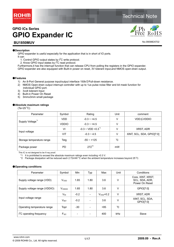
●Description GPIO expander is useful especially for the application that is in short of IO ports. It can 1. Control GPIO output states by I2C write protocol. 2. Know GPIO input states by I2C read protocol. Furthermore,it has the interrupt function that can release CPU from polling the registers in the GPIO expander. GPIO expander are also equipped with Built-in power on reset, 3V tolerant input,and NMOS open-drain output.

●Features 1) An 8-Port General purpose input/output interface 150kΩPull-down resistance. 2) NMOS Open-drain output interrupt controller with up to 1us pulse noise filter and bit mask function for individual GPIO port. 3) 3volt tolerant Input 4) Built-in Power On Reset 5) 3mmx3mm small package

●Absolute maximum ratings (Ta=25 o C)

Parameter Symbol Rating Unit comment

VDD -0.3 ~ +4.5 V VDD≦VDDIO

Supply Voltage*1

VDDIO -0.3 ~ +4.5 V VI -0.3 ~ VDD +0.3*1 V XRST, ADR

Input voltage

VIT -0.3 ~ 4.5 V XINT, SCL, SDA, GPIO[7:0]

Storage temperature range Tstg -55 ~ +125 ℃

Package power PD 272*2 m W

This IC is not designed to be X-ray proof. *1 It is prohibited to exceed the absolute maximum ratings even including +0.3 V. *2 Package dissipation will be reduced each 2.72m W/ o C when the ambient temperature increases beyond 25 o C.

●Operating conditions

Parameter Symbol Min Typ Max Unit Conditions

Core, XINT, XRST,

Supply voltage range (VDD) VVDD 1.65 1.80 3.6 V SCL, SDA, ADR,

Power On Reset

Supply voltage range (VDDIO) VVDDIO 1.65 1.80 3.6 V GPIO[7:0]

VIN -0.2 - VVDD+0.2 V XRST, ADR

Input voltage range

XINT, SCL, SDA,

VINT -0.2 - 3.6 V

GPIO[7:0]

Operating temperature range Topr -30 - +85 ℃

I2C operating frequency FI2C - - 400 k Hz Slave

www.rohm.com 2009.09 - Rev.A 1/17 © 2009 ROHM Co., Ltd. All rights reserved.

Page Summary Contents For ROHM BU1850MUV Data Sheet

Page 1 GPIO ICs Series GPIO Expander IC No.09098EAT02 BU1850MUV ●Description GPIO expander is useful especially for the application that is in short of IO ports. It can 1. Control GPIO output states by I2C w...
Page 2 BU1850MUV Technical Note ●Package Specification Lot No. (UNIT: mm) Fig.1 Package Specification (VQFN016V3030) www.rohm.com 2009.09 - Rev.A 2/17 © 2009 ROHM Co., Ltd. All rights reserved.
Page 3 BU1850MUV Technical Note ●Pin Assignment 13 GPIO4 8 VSS 14 GPIO5 7 VDDIO 15 GPIO6 6 VDD 16 GPIO7 5 SDA Fig.2 Pin Diagram (Top View) ●Block Diagram Functional Block Diagram Interrupt Interrupt XINT INT...
Page 4 BU1850MUV Technical Note ●Pin-out Functional Descriptions PIN Power source Cell PIN name I/O Function Init No. system Type 1 XINT O VDD Interrupt signal (1s pulse cut)*1 Hi-Z B (NMOS Open-drain) 2 XR...
Page 5 BU1850MUV Technical Note ●Functional Description 1. Power Modes The device enters the state of Power Down when XRST=”Low” or enters the operation state when XRST=High after powered. Refer to “Electric...
Page 6 BU1850MUV Technical Note 2. I2C Bus Interface Each function of GPIO is controlled by an internal register. The I2C Slave interface is used to write or read this internal register. The device supports ...
Page 7 BU1850MUV Technical Note 2-4 Acknowledge After start condition is occurred, 8 bits data will be transferred. SDA is latched by the rising edge of SCL. Then the “Master” opens SDA to “1” and “Slave” de...
Page 8 BU1850MUV Technical Note 2-6 Reading protocol After Writing the slave address and Read/Write commend bits, the next byte is read. The reading register address is next of previous accessed address. The...
Page 9 BU1850MUV Technical Note 3. Register configuration The address is increased one by one when data is continuously written. When the final address is set to 13h, then the next address 00h will be writte...
Page 10 BU1850MUV Technical Note 4. GPIO-Interrupt 4-1 GPIO configuration As the default value, GPIO[7:0] ports are input and Pull-down. At this time, WRSELn is "0" and XPDn is "0". (n is ...
Page 11 BU1850MUV Technical Note 4-4 Read from GPIO port After writing of the Slave address and R/W bits, reading GPIO port is begun from the following byte. The data that had been being fixed between the fol...
Page 12 BU1850MUV Technical Note ●Electrical Specification 1. DC characteristics VVDD=1.8V,VVDDIO=1.8V,Topr=25℃ Specification Parameter Symbol Unit Conditions Min Typ Max Input H Voltage1 VIH1 0.7x VVDDIO - 3...
Page 13 BU1850MUV Technical Note 3. I2C AC characteristics (Repeated) BIT 7 BIT 6 Ack STOPState START t SU;STA 1/f SCLK t HIGH t LOW t SU;DAT t SU;STO t BUF t HD;STA t HD;DAT Fig.14 I2C AC Timing VVDD=1.8V,VV...
Page 14 BU1850MUV Technical Note 4. GPIO AC Characteristics BIT 0BIT 1 Ack State Ack BIT 0BIT 1 GPIO[7:0](Output) t DS t DH GPIO[7:0](Input) t IV t IR Fig.15 GPIO AC timing VVDD=1.8V,VVDDIO=1.8V,Topr=25℃ Spec...
Page 15 BU1850MUV Technical Note 5. Startup sequence t VDD t VDD VDD, t VDD VDDIO t RWAIT t RWAIT t VDD t I2CWAIT t I2CWAIT Fig.16 Start Sequence timing VVDD=1.8V,VVDDIO=1.8V,Topr=25℃ Specification Parameter ...
Page 16 BU1850MUV Technical Note ●Application circuit example ADR ADR GPIO7 GPIO7 IN XINT GPIO6 XINT GPIO6 GPIO5 GPIO5 GPIO4 GPIO4 GPIO3 GPIO3 SCL SCL SDA GPIO2 GPIO2 SDA SDA GPIO1 GPIO1 GPIO0 GPIO0 Other I2C...
Page 17 BU1850MUV Technical Note ●Ordering part number Part No. Part No. Package Packaging and forming specification MUV: E2: Embossed tape and reel VQFN016V3030 VQFN016V3030 <Tape and Reel information>...
Page 18 Notice No copying or reproduction of this document, in part or in whole, is permitted without the consent of ROHM Co.,Ltd. The content specified herein is subject to change for improvement without not...

Manual Details

Brand ROHM
Pages 18
File Size 407.74 KB
Published June 17, 2026
1 views

Enter the captcha to get the download link:

captcha

Frequently Asked Questions

What is the max I2C operating frequency?

The maximum I2C operating frequency is 400 kHz in slave mode.

How do I reset the device?

Set XRST to Low to enter power down state and reset, or connect XRST to VDD to use built-in power on reset.

What is the operating temperature range?

The operating temperature range is -30°C to +85°C.

How many GPIO ports does this expander have?

It has an 8-port general purpose input/output interface.