# A B C D E F G H I J K L M N O P Q R S T U V W X Y Z

ROHM BD9533EKN Data Sheet

Summary

The BD9533EKN is a high-performance switching regulator controller optimized for robust power delivery to DDR-SDRAM cores in demanding computing applications. This advanced IC manages wide input voltage ranges while providing precise, low-voltage regulation through unique technologies like H Reg and SLLM efficiency mode. The accompanying manual provides comprehensive electrical specifications, detailed operating parameters, and built-in protections (OCP/OVP) required for reliable integration into modern desktop PCs, laptops, LCD TVs, and digital electronic devices.
📄 Preview PAGE OF 21

Page 1 Text Content

TECHNICAL NOTE

High-performance Regulator IC Series for PCs

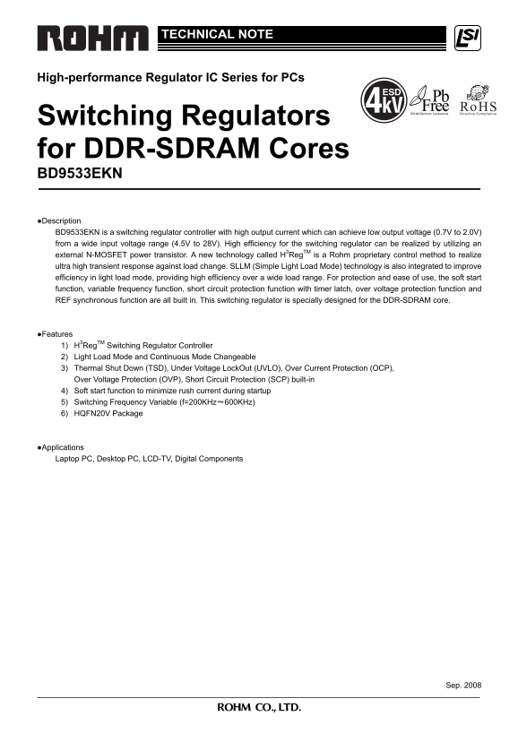
Switching Regulators for DDR-SDRAM Cores BD9533EKN ●Description BD9533EKN is a switching regulator controller with high output current which can achieve low output voltage (0.7V to 2.0V) from a wide input voltage range (4.5V to 28V). High efficiency for the switching regulator can be realized by utilizing an external N-MOSFET power transistor. A new technology called H3Reg TM is a Rohm proprietary control method to realize ultra high transient response against load change. SLLM (Simple Light Load Mode) technology is also integrated to improve efficiency in light load mode, providing high efficiency over a wide load range. For protection and ease of use, the soft start function, variable frequency function, short circuit protection function with timer latch, over voltage protection function and REF synchronous function are all built in. This switching regulator is specially designed for the DDR-SDRAM core.

●Features 1) H3Reg TM Switching Regulator Controller 2) Light Load Mode and Continuous Mode Changeable 3) Thermal Shut Down (TSD), Under Voltage Lock Out (UVLO), Over Current Protection (OCP), Over Voltage Protection (OVP), Short Circuit Protection (SCP) built-in 4) Soft start function to minimize rush current during startup 5) Switching Frequency Variable (f=200KHz~600KHz) 6) HQFN20V Package

●Applications Laptop PC, Desktop PC, LCD-TV, Digital Components

Sep. 2008

Page Summary Contents For ROHM BD9533EKN Data Sheet

Page 1 TECHNICAL NOTE High-performance Regulator IC Series for PCs Switching Regulators for DDR-SDRAM Cores BD9533EKN ●Description BD9533EKN is a switching regulator controller with high output current which...
Page 2 ●Maximum Absolute Ratings (Ta=25℃) Parameter Symbol Limit Unit Input Voltage 1 VCC 7 *1 Input Voltage 2 VDD 7 *1 Input Voltage 3 VIN 30 *1 BOOT Voltage BOOT 35 *1 BOOT-SW Voltage BOOT-SW 7 *1 HG-SW Vo...
Page 3 ●ELECTRICAL CHARACTERISTICS (unless otherwise noted, Ta=25℃ VCC=5V,VDD=5V,EN/SLLM=5V,VIN=12V,REF=1.8V,RFS=68kΩ) Standard Value Parameter Symbol Unit Condition MIN TYP MAX [Whole Device] VCC Bias Curre...
Page 4 ●Reference Data ns ec IN [V (V cc (u 2.498 Sweep up 4.10 Sweep down Ta(℃) Ta(℃) Ta(℃) Fig.1 Ta vs Icc Fig.3 Ta vs UVLO (VCC) Fig.2 Ta vs VREG se c] [V ns ec Sweep up 1.6 Sweep up Sweep up Sweep down S...
Page 5 ●Reference Data Io=2A Io=0A ILIM=0.5V Ta(℃) VIN(V) Te [℃] Fig.13 Ta vs current limit Fig.14 Ta vs Frequency Fig.15 VIN vs Frequency fr eq ue nc y[ k H z] threshould Continuous mode Continuous Continuo...
Page 6 ●Reference Data VOUT VOUT IL IL HG/LG HG/LG HG/LG Fig.25 SLLM Fig.26 SLLM Fig.27 SLLM (IOUT=0A) (IOUT=0.4A) (IOUT=1A) re cy k H z] IL IL IL HG/LG/SW HG/LG/SW HG/LG/SW Fig.28 Continuous MODE Fig.29 Con...
Page 7 ●Block Diagram SS VREGVIN VCC UVLO VREG Reference SS Block 2.5VReg Soft Start Block REF×1.2 REF×0.7 SCP SS×0.7 SCP SCP HG VOUT Driver H3Reg TM SLLMR SW Circuit REF Controller VDD Block SS Current Limi...
Page 8 ●Pin Descriptions ・GND(1pin) This is the ground pin for IC internal circuits. It is equivalent to FIN voltage. ・VCC(2pin) This is the power supply pin for IC internal circuits, except the FET driver. ...
Page 9 ●Explanation of Operation The BD9533EKN is a synchronous buck regulator controller incorporating ROHM’s proprietary H3Reg TM CONTROLLA control system. When VOUT drops due to a rapid load change, the s...
Page 10 ●Timing Chart • Soft Start Function Soft start is exercised with the EN pin set high. Current EN control takes effect at startup, enabling a moderate output voltage “ramping start.” Soft start timing ...
Page 11 ●External Component Selection 1. Inductor (L) selection The inductor value is a major influence on the output ripple current. As formula (5) below indicates, the greater the inductor or the switching ...
Page 12 4. MOSFET Selection Loss on the main MOSFET Pmain=PRON+PGATE+PTRAN main switch VOUT 2+Ciss×f×VDD+ VIN ×Crss×IOUT×f ×RON×IOUT ・・・(11) VIN IDRIVE Co (Ron: On-resistance of FET; Ciss: FET gate capacity; ...
Page 13 6.Setting frequency On Time (TON) at steady state is determined by ns ec VIN=5V re qu en cy k H z] resistance value connected to FS pin as shown in the 12V figure. The frequency can be calculated with...
Page 14 8. Setting output voltage This IC is operated that output voltage is REF≒VOUT. And it is operated that output voltage is feed back to FB pin in case the output voltage is 0.7V to 2.0V. VIN VIN Output ...
Page 15 ●I/O Equivalent Circuit 3pin (ILIM) 4pin (EN) 5pin (VIN) 6pin (SLLM) 7pin (SCP) 8pin (Is-) VCC VCC VCC 9pin (Is+) 11pin (LG) 13pin (SW) BOOT HG VCC VCC 14pin(HG) 15pin (BOOT) 16pin (SS) BOOT BOOT HG S...
Page 16 ●Evaluation Board Circuit (Frequency=300k Hz application circuit in Continuous mode/SLLM) 4.5V~25V VIN BD9533EKN VIN VDD EN R18 SLLM PGND VREG R10 Q1 PGND PGND 2.5V HG VOUT VREG 1.8V/10A ILIM R6 REF 1...
Page 17 ●Evaluation Board Circuit (Frequency=300k Hz application circuit for detecting DCR current in Continuous mode/SLLM) 4.5V~25V VIN BD9533EKN VIN VDD EN R18 SLLM PGND VREG R10 PGND PGND HG VOUT ILIM R6 R...
Page 18 ●Operation Notes 1. Absolute maximum ratings An excess in the absolute maximum ratings, such as supply voltage, temperature range of operating conditions, etc., can break down the devices, thus making...
Page 19 11. Regarding input pin of the IC This monolithic IC contains P+ isolation and P substrate layers between adjacent elements in order to keep them isolated. P-N junctions are formed at the intersection...
Page 20 ●Type Designations (Selections) for Ordering Product name Package type Taping type name ・BD9533 ・EKN : HQFN20V E2= Embossed carrier tape HQFN20V <Dimension> <Tape and Reel information> Tap...
Page 21 Appendix Notes No copying or reproduction of this document, in part or in whole, is permitted without the consent of ROHM CO.,LTD. The content specified herein is subject to change for improvement wit...

Manual Details

Brand ROHM
Pages 21
File Size 719.80 KB
Published June 17, 2026
2 views

Enter the captcha to get the download link:

captcha

Frequently Asked Questions

What is the input voltage range of BD9533EKN?

The input voltage VIN range is 4.5V to 28V, with VCC and VDD at 4.5V to 5.5V.

What protection features does this regulator have?

It has TSD, UVLO, OCP, OVP, SCP with timer latch, and overcurrent protection.

What is the switching frequency range of BD9533EKN?

The switching frequency is variable from 200KHz to 600KHz.

Can this regulator be used in medical devices?

No, it is not designed for medical or other high-reliability safety-critical equipment.