# A B C D E F G H I J K L M N O P Q R S T U V W X Y Z

ROHM BD8163EFV Data Sheet

Summary

The BD8163EFV is a versatile system power supply IC designed for TFT-LCD panels. Supporting a 5V input, it efficiently generates logic, sauce, and gate voltages using a step-up DC/DC converter and charge pumps. Ideal for liquid crystal TVs, PC monitors, and electronics, this chip offers robust protection features and compact HTSSOP-B24 packaging.
📄 Preview PAGE OF 22

Page 1 Text Content

Power Supply ICs for TFT-LCD Panels

5V Input Multi-channel System Power Supply ICs

No.10035EAT13

BD8163EFV

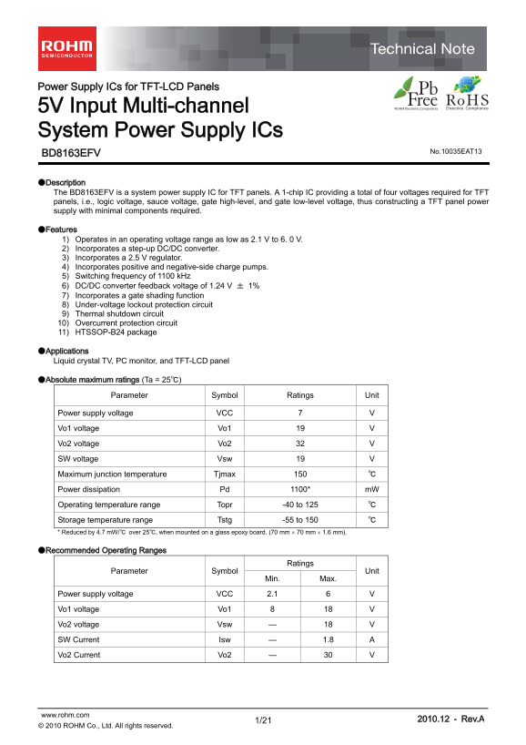
●Description The BD8163EFV is a system power supply IC for TFT panels. A 1-chip IC providing a total of four voltages required for TFT panels, i.e., logic voltage, sauce voltage, gate high-level, and gate low-level voltage, thus constructing a TFT panel power supply with minimal components required.

●Features 1) Operates in an operating voltage range as low as 2.1 V to 6. 0 V. 2) Incorporates a step-up DC/DC converter. 3) Incorporates a 2.5 V regulator. 4) Incorporates positive and negative-side charge pumps. 5) Switching frequency of 1100 k Hz 6) DC/DC converter feedback voltage of 1.24 V ± 1% 7) Incorporates a gate shading function 8) Under-voltage lockout protection circuit 9) Thermal shutdown circuit 10) Overcurrent protection circuit 11) HTSSOP-B24 package

●Applications Liquid crystal TV, PC monitor, and TFT-LCD panel

●Absolute maximum ratings (Ta = 25℃)

Parameter Symbol Ratings Unit

Power supply voltage VCC 7 V Vo1 voltage Vo1 19 V Vo2 voltage Vo2 32 V SW voltage Vsw 19 V Maximum junction temperature Tjmax 150 ℃ Power dissipation Pd 1100* m W Operating temperature range Topr -40 to 125 ℃ Storage temperature range Tstg -55 to 150 ℃ * Reduced by 4.7 m W/℃ over 25℃, when mounted on a glass epoxy board. (70 mm  70 mm  1.6 mm).

●Recommended Operating Ranges

Ratings

Parameter Symbol Unit

Min. Max.

Power supply voltage VCC 2.1 6 V Vo1 voltage Vo1 8 18 V Vo2 voltage Vsw — 18 V SW Current Isw — 1.8 A Vo2 Current Vo2 — 30 V

www.rohm.com 2010.12 - Rev.A

© 2010 ROHM Co., Ltd. All rights reserved.

Page Summary Contents For ROHM BD8163EFV Data Sheet

Page 1 Power Supply ICs for TFT-LCD Panels 5V Input Multi-channel System Power Supply ICs No.10035EAT13 BD8163EFV ●Description The BD8163EFV is a system power supply IC for TFT panels. A 1-chip IC providing ...
Page 2 BD8163EFV Technical Note ●Electrical Characteristics (Unless otherwise specified, VCC = 5 V; Vo1 = 15 V; Vo2 = 25 V; Ta = 25℃) 1 DC/DC Converter Block Limits Parameter Symbol Unit Conditions Min. Typ....
Page 3 BD8163EFV Technical Note 3. Charge pump Limits Parameter Symbol Unit Conditions Min. Typ. Max. [Error amp] Input bias current 2 IFB2 — 0.1 0.5 μA Input bias current 3 IFB3 — 0.1 0.5 μA Feedback voltag...
Page 4 BD8163EFV Technical Note 4. Overall Limits Parameter Symbol Unit Conditions Min. Typ. Max. [Reference block] Reference voltage VREF 1.215 1.240 1.265 V Drive current IREF — 23 — m A VREF = 0 V Load re...
Page 5 BD8163EFV Technical Note LT [V LT [V IC [m LS ID LS [µ ●Reference Data (Unless otherwise specified, Ta = 25℃) SUPPLY VOLTAGE : VCC [V] SUPPLY VOLTAGE : VDD[V] AMBIENT TEMPERATURE : Ta[℃] Fig. 1 Total ...
Page 6 BD8163EFV Technical Note IM Io [m LT 3[ LT 1[ LT [V ●Reference Data (Unless otherwise specified, Ta = 25℃) SUPPLY VOLTAGE : VCC [V] OUTPUT CURRENT : IDD[m A] SUPPLY VOLTAGE : VCC[V] Fig. 13 Vo1 Line R...
Page 7 BD8163EFV Technical Note ●Block Diagram VCC 10µF 5V Vo1=14.5V (18V MAX) VCC SW Vo1 Step-up SS FB1 15kΩ Controller COMP Vo1 Vo2 Vo2 23.5V (30V MAX) Charge Vo1 C1H Control 1 TSD UVLO Step-up Controller ...
Page 8 BD8163EFV Technical Note ●Pin Assignments Diagram GND REF VDD FB3 VCC C3 DLS Vo1 COMP C1H FB1 C1L SS C2L PGND C2H SW GSOUT IG Vo2GS FB2 Vo2 Pin Arrangements ●Pin Assignments and Function PIN Pin PIN P...
Page 9 BD8163EFV Technical Note ●Block Function ・Step-up Controller A controller circuit for DC/DC boosting. The switching duty is controlled so that the feedback voltage FB1 is set to 1.24 V (typ.). A soft ...
Page 10 BD8163EFV Technical Note ●Selecting Application Components (1) Setting the Output L Constant The coil to use for output is decided by the rating current ILR and input current maximum value IINMAX of t...
Page 11 BD8163EFV Technical Note (4) Setting RC, CC of the Phase Compensation Circuit In the current mode control, since the coil current is controlled, a pole (phase lag) made by the CR filter composed of th...
Page 12 BD8163EFV Technical Note (5) Regulator Controller Settings The IC incorporates a 2.5 V regulator controller, and a regulator can be formed by using an external PNP transistor. Design the current capab...
Page 13 BD8163EFV Technical Note (6) Setting the Soft Start Time Soft start is required to prevent the coil current at the time of start from increasing and the overshoot of the output voltage at the starting...
Page 14 BD8163EFV Technical Note (8) Positive-side Charge Pump Settings The IC incorporates a charge pump controller, thus making it possible to generate stable gate voltage. The output voltage is determined ...
Page 15 BD8163EFV Technical Note ●Gate Shading Setting Method The IG input signal allows the high-level and low-level control of the positive-side gate voltage. The slope of output can be set by the external ...
Page 16 BD8163EFV Technical Note ●Application Examples Although we are confident that the application circuit diagram reflects the best possible recommendations, be sure to verify circuit characteristics for ...
Page 17 BD8163EFV Technical Note (c) When Inserting PMOS Switch Vo2GS Vo2 VDD Vo1 Fig. 42 www.rohm.com 2010.12 - Rev.A © 2010 ROHM Co., Ltd. All rights reserved.
Page 18 BD8163EFV Technical Note ●I/O Equivalent Circuits 2.VDD 3.BASE 5.DLS,8.SS 6.COMP 7.FB1,12.FB2 10.SW VDD VDD 11.IG 13.Vo2 14.Vo2GS VDD VDD Vo2 15.GSOUT 16.C2H,19.C1H 17.C2L,18.C1L,21.C3 Vo2 Vo1 Vo1 23....
Page 19 BD8163EFV Technical Note ●Power Dissipation Reduction On 70 mm mm 1.6 mm Glass-epoxy PCB ow er is si pa tio (m Ambient Temperature: Ta(℃) Fig.44 ●Notes for use 1) Absolute maximum ratings Use of the I...
Page 20 BD8163EFV Technical Note 8) This monolithic IC contains P+ isolation and P substrate layers between adjacent elements in order to keep them isolated. P/N junctions are formed at the intersection of th...
Page 21 BD8163EFV Technical Note ●Ordering part number Part No. Part No. Package Packaging and forming specification EFV: HTSSOP-B24 E2: Embossed tape and reel HTSSOP-B24 (3 .4 <Tape and Reel information&g...
Page 22 Notice No copying or reproduction of this document, in part or in whole, is permitted without the consent of ROHM Co.,Ltd. The content specified herein is subject to change for improvement without not...

Manual Details

Brand ROHM
Pages 22
File Size 511.33 KB
Published June 16, 2026
1 views

Enter the captcha to get the download link:

captcha

Frequently Asked Questions

What input voltage range does the BD8163EFV support?

It operates from 2.1 V to 6.0 V.

What does the IC protect against?

It has under-voltage lockout, thermal shutdown, and overcurrent protection circuits.

What package does the BD8163EFV come in?

It uses an HTSSOP-B24 package.