# A B C D E F G H I J K L M N O P Q R S T U V W X Y Z

ROHM BD8157EFV Data Handbook/Specifications Sheet

Summary

Discover this integrated Power Supply IC series, featuring a sophisticated single-chip design that combines source voltage step-up regulation with a gamma correction buffer amplifier for TFT-LCD panels. Manual specifications detail its excellent low-voltage performance and high efficiency (>85%), supporting input voltages from 2.1 V to 5.5 V. Designed for minimal power usage, this module is essential for applications like laptop LCDs, satellite navigation systems, and general monitor displays, ensuring reliable and comprehensive power management in modern electronics.
📄 Preview PAGE OF 18

Page 1 Text Content

Power Supply IC Series for TFT-LCD Panels

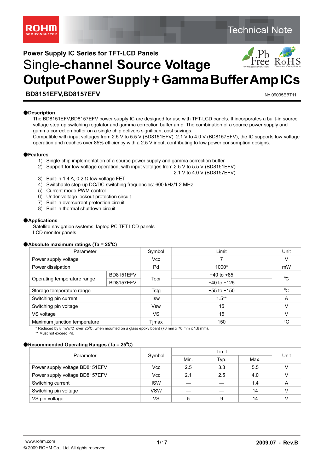
ingle S -channel Source Voltage Output Power Supply + Gamma Buffer Amp ICs BD8151EFV,BD8157EFV No.09035EBT11 ●Description The BD8151EFV,BD8157EFV power supply IC are designed for use with TFT-LCD panels. It incorporates a built-in source voltage step-up switching regulator and gamma correction buffer amp. The combination of a source power supply and gamma correction buffer on a single chip delivers significant cost savings. Compatible with input voltages from 2.5 V to 5.5 V (BD8151EFV), 2.1 V to 4.0 V (BD8157EFV), the IC supports low-voltage operation and reaches over 85% efficiency with a 2.5 V input, contributing to low power consumption designs. ●Features 1) Single-chip implementation of a source power supply and gamma correction buffer 2) Support for low-voltage operation, with input voltages from 2.5 V to 5.5 V (BD8151EFV)

2.1 V to 4.0 V (BD8157EFV)

3) Built-in 1.4 A, 0.2  low-voltage FET 4) Switchable step-up DC/DC switching frequencies: 600 k Hz/1.2 MHz 5) Current mode PWM control 6) Under-voltage lockout protection circuit 7) Built-in overcurrent protection circuit 8) Built-in thermal shutdown circuit

●Applications Satellite navigation systems, laptop PC TFT LCD panels LCD monitor panels

●Absolute maximum ratings (Ta = 25℃)

Parameter Symbol Limit Unit

Power supply voltage Vcc 7 V Power dissipation Pd 1000* m W

BD8151EFV −40 to +85

Operating temperature range Topr

BD8157EFV −40 to +125

Storage temperature range Tstg −55 to +150 ℃ Switching pin current Isw 1.5** A Switching pin voltage Vsw 15 V VS voltage VS 15 V Maximum junction temperature Tjmax 150 °C * Reduced by 8 m W/℃ over 25℃, when mounted on a glass epoxy board (70 mm x 70 mm x 1.6 mm). ** Must not exceed Pd.

●Recommended Operating Ranges (Ta = 25℃)

Limit

Parameter Symbol Unit

Min. Typ. Max.

Power supply voltage BD8151EFV Vcc 2.5 3.3 5.5 V Power supply voltage BD8157EFV Vcc 2.1 2.5 4.0 V Switching current ISW — — 1.4 A Switching pin voltage VSW — — 14 V VS pin voltage VS 5 9 14 V

1/17 www.rohm.com 2009.07 - Rev.B

© 2009 ROHM Co., Ltd. All rights reserved.

Page Summary Contents For ROHM BD8157EFV Data Handbook/Specifications Sheet

Page 1 Power Supply IC Series for TFT-LCD Panels ingle S -channel Source Voltage Output Power Supply + Gamma Buffer Amp ICs BD8151EFV,BD8157EFV No.09035EBT11 ●Description The BD8151EFV,BD8157EFV power supply...
Page 2 BD8151EFV, BD8157EFV Technical Note ●Electrical Characteristics BD8151EFV (Unless otherwise specified, Ta = 25℃; Vcc = 3.3V, ENB = 3.3V) Limit Parameter Symbol Unit Conditions Min. Typ. Max. [Triangul...
Page 3 BD8151EFV, BD8157EFV Technical Note ●Electrical Characteristics BD8157EFV (Unless otherwise specified, Ta = 25℃; Vcc = 2.5V, ENB = 2.5V) Limit Parameter Symbol Unit Conditions Min. Typ. Max. [Triangul...
Page 4 BD8151EFV, BD8157EFV Technical Note [μ LY : I [m ax ut ●Reference Data (Unless otherwise specified, Ta = 25℃) SUPPLY VOLTAGE : VCC[V] SUPPLY VOLTAGE : VCC[V] AMBIENT TEMPERATURE : Ta[℃] [μ IC IE LT [V...
Page 5 BD8151EFV, BD8157EFV Technical Note LA IM s] :V [m IC IE ●Reference Data (Unless otherwise specified, Ta = 25℃) LT [V BD8157EFV Io=0m A Io=100m A F=600k Hz F=1200k Hz 100m V/div 20us/div BD8157EFV SUP...
Page 6 BD8151EFV, BD8157EFV Technical Note ●Pin Assignment Diagram ●Block Diagram SW PGND CURRENT SENSE VCC GND SLOPE SW PGND ENB SET LOGIC FB GND OSC VCC RESET SDWN OCP ENB FB FCLK COMP FCLK COMP UVLO TSD P...
Page 7 BD8151EFV, BD8157EFV Technical Note ●Description of Operation of Each Block 10u H Vo RB161M-20 10u F SW PGND CURRENT SENSE 10u F VCC 2.5V VCC SLOPE GND 100kΩ SET LOGIC ERR OSC 15kΩ ENB RESET SDWN OCP ...
Page 8 BD8151EFV, BD8157EFV Technical Note ●Timing Chart Startup sequence Fig. 27 Startup sequence Overcurrent protection operating VCC,ENB Fig. 28 Overcurrent protection operating 8/17 www.rohm.com 2009.07 ...
Page 9 BD8151EFV, BD8157EFV Technical Note ●Selecting Application Components (1) Setting the output L constant The coil L to use for output is decided by the rating current ILR and input current maximum valu...
Page 10 BD8151EFV, BD8157EFV Technical Note (4) Selecting the output rectification diode Schottky barrier diode is recommended as the rectification diode to use at the DC/DC converter output stage. Select the...
Page 11 BD8151EFV, BD8157EFV Technical Note (9) Setting RC, CC of the phase compensation circuit In the current mode control, since the coil current is controlled, a pole (phase lag) made by the CR filter com...
Page 12 BD8151EFV, BD8157EFV Technical Note (10) Using the buffer amp and VCOM The 4-channel buffer amp and 1-channel VCOM output are used to generate the gamma compensation voltage that is input to the sourc...
Page 13 BD8151EFV, BD8157EFV Technical Note ●Application Examples * Although ROHM is sure that the application examples are recommendable ones, further check the characteristics of components that require hig...
Page 14 BD8151EFV, BD8157EFV Technical Note ●I/O Equivalent Circuit Diagrams 1.SW 11.OUT4 12.OUT3 13.OUT2 14.OUT1 15.VCOM 3.ENB 4.FCLK 16.SS 6.COMIN 7.IN1 8.IN2 9.IN3 10.IN4 17.COMP 18.FB Fig.40 I/O Equivalen...
Page 15 BD8151EFV, BD8157EFV Technical Note ●Notes for use 1) Absolute maximum ratings Use of the IC in excess of absolute maximum ratings such as the applied voltage or operating temperature range may result...
Page 16 BD8151EFV, BD8157EFV Technical Note ●Power Dissipation Reduction On 70×70×1.6mm Board IS IP IO BD8151EF BD8157EF AMBIENT MPERATURE :Ta[℃] Fig.42 Power Dissipation Reduction 16/17 www.rohm.com 2009.07 ...
Page 17 BD8151EFV, BD8157EFV Technical Note ●Ordering part number Part No. Part No. Package Packaging and forming specification EFV : HTSSOP-B20 E2: Embossed tape and reel HTSSOP-B20 <Tape and Reel informa...
Page 18 Notice No copying or reproduction of this document, in part or in whole, is permitted without the consent of ROHM Co.,Ltd. The content specified herein is subject to change for improvement without not...

Manual Details

Brand ROHM
Pages 18
File Size 505.04 KB
Published July 07, 2026
3 views

Enter the captcha to get the download link:

captcha

Frequently Asked Questions

What input voltages are supported by the BD8151EFV and BD8157EFV ICs?

The BD8151EFV supports 2.5 V to 5.5 V, while the BD8157EFV supports 2.1 V to 4.0 V.

What is a key benefit of using these single-chip power supply ICs?

They incorporate both the source voltage step-up regulator and gamma correction buffer on one chip, offering cost savings.

Do these ICs have protective features built in?

Yes, they include under-voltage lockout, overcurrent protection, and thermal shutdown circuits.

What is the maximum operating temperature range for both IC models?

The BD8151EFV has an operating range of -40 to +85℃, and the BD8157EFV ranges from -40 to +125℃.