# A B C D E F G H I J K L M N O P Q R S T U V W X Y Z

ROHM BD8139AEFV Data Sheet

Summary

Achieve optimized display performance with these high-precision Gamma Correction Power Supply ICs. This advanced single-chip solution integrates a built-in 10-bit DAC and necessary amplifier blocks, making them ideal for modern large-screen and high-definition TFT-LCD TV panels. The accompanying manual provides comprehensive technical documentation, including absolute maximum ratings, detailed electrical characteristics, operational ranges, and application guidance, strictly for hardware engineers and system designers integrating advanced LCD display technology.
📄 Preview PAGE OF 21

Page 1 Text Content

Power Supply IC Series for TFT-LCD Panels

High-precision Gamma Correction ICs with built-in DAC

BD8132FV, BD8139AEFV No.09035EBT02

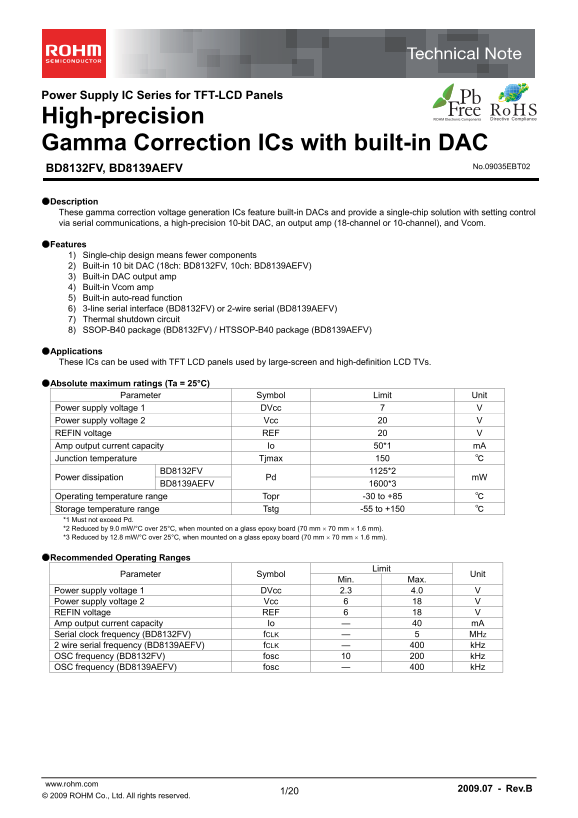
●Description These gamma correction voltage generation ICs feature built-in DACs and provide a single-chip solution with setting control via serial communications, a high-precision 10-bit DAC, an output amp (18-channel or 10-channel), and Vcom.

●Features 1) Single-chip design means fewer components 2) Built-in 10 bit DAC (18ch: BD8132FV, 10ch: BD8139AEFV) 3) Built-in DAC output amp 4) Built-in Vcom amp 5) Built-in auto-read function 6) 3-line serial interface (BD8132FV) or 2-wire serial (BD8139AEFV) 7) Thermal shutdown circuit 8) SSOP-B40 package (BD8132FV) / HTSSOP-B40 package (BD8139AEFV)

●Applications These ICs can be used with TFT LCD panels used by large-screen and high-definition LCD TVs.

●Absolute maximum ratings (Ta = 25°C)

Parameter Symbol Limit Unit

Power supply voltage 1 DVcc 7 V Power supply voltage 2 Vcc 20 V REFIN voltage REF 20 V Amp output current capacity Io 50*1 m A Junction temperature Tjmax 150 ℃

BD8132FV 1125*2

Power dissipation Pd m W

BD8139AEFV 1600*3

Operating temperature range Topr -30 to +85 ℃ Storage temperature range Tstg -55 to +150 ℃ *1 Must not exceed Pd. *2 Reduced by 9.0 m W/°C over 25°C, when mounted on a glass epoxy board (70 mm  70 mm  1.6 mm). *3 Reduced by 12.8 m W/°C over 25°C, when mounted on a glass epoxy board (70 mm  70 mm  1.6 mm).

●Recommended Operating Ranges

Limit

Parameter Symbol Unit

Min. Max.

Power supply voltage 1 DVcc 2.3 4.0 V Power supply voltage 2 Vcc 6 18 V REFIN voltage REF 6 18 V Amp output current capacity Io — 40 m A Serial clock frequency (BD8132FV) f CLK — 5 MHZ 2 wire serial frequency (BD8139AEFV) f CLK — 400 k Hz OSC frequency (BD8132FV) fosc 10 200 k Hz OSC frequency (BD8139AEFV) fosc — 400 k Hz

www.rohm.com 2009.07 - Rev.B

© 2009 ROHM Co., Ltd. All rights reserved.

Page Summary Contents For ROHM BD8139AEFV Data Sheet

Page 1 Power Supply IC Series for TFT-LCD Panels High-precision Gamma Correction ICs with built-in DAC BD8132FV, BD8139AEFV No.09035EBT02 ●Description These gamma correction voltage generation ICs feature bu...
Page 2 BD8132FV, BD8139AEFV Technical Note ●Electrical Characteristics BD8132FV(Unless otherwise specified, Vcc = 15 V, DVcc = 3.3 V, Ta = 25℃) Limit Parameter Symbol Unit Condition Min. Typ. Max. [REFIN] Si...
Page 3 BD8132FV, BD8139AEFV Technical Note ●Electrical Characteristics BD8139AEFV (Unless otherwise specified, Vcc = 15 V, DVcc = 3.3 V, Ta = 25℃) Limit Parameter Symbol Unit Condition Min. Typ. Max. [REFIN]...
Page 4 BD8132FV, BD8139AEFV Technical Note LY [m LT [V LY [m ●Reference Data (Unless otherwise specified, Ta = 25℃, BD8132FV and BD8139AEFV) BD8132FV BD8132FV BD8132FV -30 -10 IC [m LY [m LT [V SUPPLY VOLTAG...
Page 5 BD8132FV, BD8139AEFV Technical Note ut pu t V ol ta ge [V ai [d ut pu t V ol ta ge [V ●Reference Data (Unless otherwise specified, Ta = 25℃, BD8132FV and BD8139AEFV) Phase In pu t C ur re nt ha se [d ...
Page 6 BD8132FV, BD8139AEFV Technical Note ●Pin Assignment Diagram ●Block Diagram [BD8132FV] REFIN VDAC VCC DVCC 100kΩ VREF 100kΩ V0 VCC LATCH V0 Register 0 SDIN V1 TSD V1 Register 1 ×2 VDAC ×2 V2 V3 Registe...
Page 7 BD8132FV, BD8139AEFV Technical Note ●Pin Assignment Diagram ●Block Diagram [BD8139AEFV] REFIN VDAC Vcc GND 100kΩ DVcc VDAC A2 NC 100kΩ VCC NC NC VREF V0 Register 0 OSC NC ×2 V1 Register 1 SLAVE/AR V0 ...
Page 8 BD8132FV, BD8139AEFV Technical Note ●Block Operation ・VDAC Amp The VDAC Amp amplifies the voltage applied to REFIN by 0.5x and outputs it to the VDAC pin. Connect a 1 µF phase compensation capacitor t...
Page 9 BD8132FV, BD8139AEFV Technical Note [BD8132FV] ●Serial communications The serial data control block consists of a register that stores data from the LATCH, CLK, and SDIN pins, and a DAC circuit that r...
Page 10 BD8132FV, BD8139AEFV Technical Note ●Auto-read function The auto-read function enables the IC's 1 kbit microwire type external memory to be automatically read. This block operates in synchronization w...
Page 11 BD8132FV, BD8139AEFV Technical Note ●Timing standard values Limit Parameter Symbol Unit Min. Typ. Max. Latch setup time t LC 0.1 — — µs SDIN setup time t SC 0.1 — — µs RW setup time t RC 0.1 — — µs ME...
Page 12 BD8132FV, BD8139AEFV Technical Note [BD8139AEFV] ●Serial communications The 2 wire serial control block consists of a register that stores data from the SCL and SDA pins and a DAC circuit that receive...
Page 13 BD8132FV, BD8139AEFV Technical Note ●SDA serial data map SLAVE mode(SLAVE/AR=L) First (MSB) Last (LSB) 1 Device address (11101<A2><A1>) 0 2 Don’t Care Register address 3 data(9:3) PC 4 dat...
Page 14 BD8132FV, BD8139AEFV Technical Note ●Timing Chart Fig. 31 2-wire serial Timing Chart (Auto-Read) Only the EEPROM device address A3 = A2 = A1 = low is supported. The auto-read function specifies the re...
Page 15 BD8132FV, BD8139AEFV Technical Note ●Timing standard values FAST-MODE Parameter Symbol 2.3 V ≤ DVCC ≤ 4.0 V Unit Min. Typ. Max. SCL frequency f SCL — — 400 k Hz SCL high time t HIGH 0.6 — — µs SCL low...
Page 16 BD8132FV, BD8139AEFV Technical Note ●Closing time for auto-read (Input VCC ~ Beginning auto-read ~ Taking time for auto-read, when 2use.) 0.9DVcc Auto-read for one Auto-read for other 0.9Vout (First g...
Page 17 BD8132FV, BD8139AEFV Technical Note ●When it inputs VCC, it outputted the gamma output voltage. 0.9Vcc 0.1Vcc t Vcc tref Tref Fig. 36 DAC 1ch supports all gamma output amps by sample/hold function. So...
Page 18 BD8132FV, BD8139AEFV Technical Note ●Input equivalent circuit diagrams [BD8132FV] 1.LATCH 2.SDIN 3.CLK 4.SDOUT 7.CS 8.MEMDO 10.OSC 15.REFIN 6.RW 9.MEMDI DVCC VCC GND GND GND GND 16.VDAC 17.CT 21.FB 2...
Page 19 BD8132FV, BD8139AEFV Technical Note ●Notes for use 1) Absolute maximum ratings Use of the IC in excess of absolute maximum ratings such as the applied voltage or operating temperature range may result...
Page 20 BD8132FV, BD8139AEFV Technical Note ●Ordering part number 1. 0M ax 7. 8± 0. Part No. Part No. Package Packaging and forming specification 8132 : 3-line serial FV: SSOP-B40 E2: Embossed tape and reel 8...
Page 21 Notice No copying or reproduction of this document, in part or in whole, is permitted without the consent of ROHM Co.,Ltd. The content specified herein is subject to change for improvement without not...

Manual Details

Brand ROHM
Pages 21
File Size 595.42 KB
Published June 18, 2026
1 views

Enter the captcha to get the download link:

captcha

Frequently Asked Questions

What is the primary function of these ICs?

They are gamma correction voltage generation ICs that provide a single-chip solution with built-in DAC and output amplification.

What panel types are these ICs suitable for?

TFT LCD panels utilized in large-screen and high-definition LCD TVs.

What are the recommended working voltage limits?

Vcc should be between 6V and 18V; DVcc should be between 2.3V and 4.0V.

Can these parts be used in life support systems?

No, they are not designed for equipment requiring an extremely high level of reliability or a direct threat to human life.