Page 1
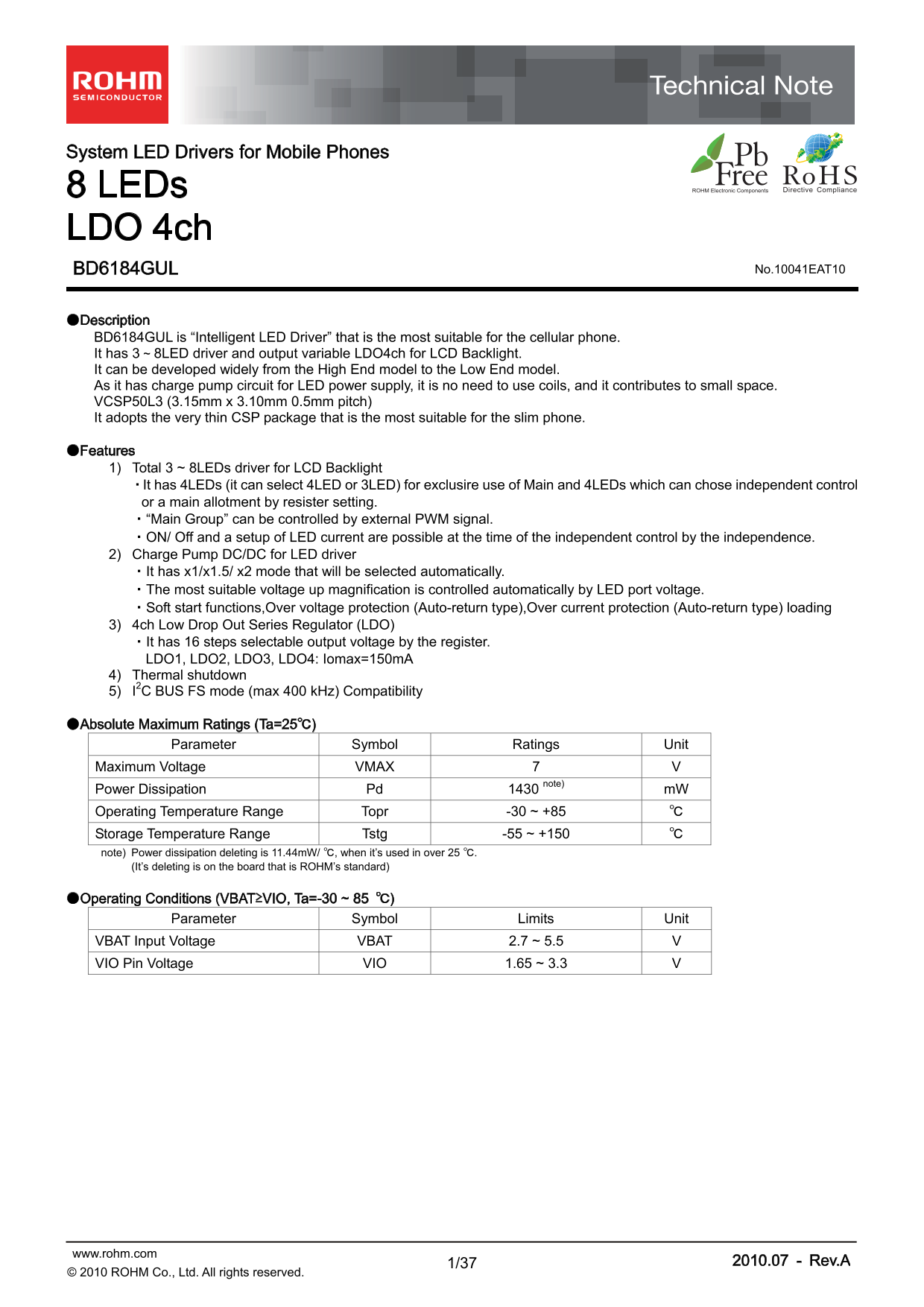
System LED Drivers for Mobile Phones 8 LEDs LDO 4ch BD6184GUL No.10041EAT10 ●Description BD6184GUL is “Intelligent LED Driver” that is the most suitable for the cellular phone. It has 3 ~ 8LED driver ...
Page 2
BD6184GUL Technical Note ●Electrical Characteristics (Unless otherwise specified, Ta=25℃, VBAT=3.6V, VIO=1.8V) Limits Parameter Symbol Unit Conditions Min. Typ. Max. 【Circuit Current】 VBAT Circuit Cur...
Page 3
BD6184GUL Technical Note ●Electrical Characteristics (Unless otherwise specified, Ta=25℃, VBAT=3.6V, VIO=1.8V) Limits Parameter Symbol Unit Conditions Min. Typ. Max. 【Regulator (LDO1)】 1.164 1.20 1.23...
Page 4
BD6184GUL Technical Note ●Electrical Characteristics (Unless otherwise specified, Ta=25℃, VBAT=3.6V, VIO=1.8V) Limits Parameter Symbol Unit Conditions Min. Typ. Max. 【Regulator (LDO3)】 1.164 1.20 1.23...
Page 5
BD6184GUL Technical Note ●Electrical Characteristics (Unless otherwise specified, Ta=25℃, VBAT=3.6V, VIO=1.8V) Limits Parameter Symbol Unit Condition Min. Typ. Max. 【SDA, SCL】(I2C Interface) L level I...
Page 6
BD6184GUL Technical Note ●Block Diagram / Application Circuit Example 1 VBATCP VBAT1 Charge Pump 2.2µF/10V LED1 Charge Pump OVP Mode Control LED terminal voltage feedback VIO LED4 ( ) ( ) 8LED RESETB ...
Page 7
BD6184GUL Technical Note ●Block Diagram / Application Circuit Example 2 VBATCP VBAT1 Charge Pump OVP LED2 Charge Pump Mode Control LED terminal voltage feedback LED3 ( ) ( ) Main Back Light RESETB (O ...
Page 8
BD6184GUL Technical Note ●Block Diagram / Application Circuit Example 3 VBATCP VBAT1 Charge Pump OVP LED2 Charge Pump Mode Control LED terminal voltage feedback LED3 Main Back Light ( ) ( ) RESETB (O ...
Page 9
BD6184GUL Technical Note ●Pin Arrangement [Bottom View] F T4 LDO4O LDO3O LDO2O LDO1O T3 E LED7 LED8 GND2 VBAT1 VIO SCL D LED6 LEDGND NC2 NC3 SDA VOUT Index C LED5 LED4 NC1 C1P C2P B LED3 LED2 GND1 RES...
Page 10
BD6184GUL Technical Note ●Package Outline VCSP50L3 CSP small package SIZE : 3.15mm x 3.10mm(A difference in public:X,Y Both ±0.05mm) Height : 0.55mm max A ball pitch : 0.5 mm 1PIN MARK Lot No. BD6184 ...
Page 11
BD6184GUL Technical Note ●Pin Functions ESD Diode No Ball No. Pin Name I/O Functions Equivalent Circuit For Power For Ground 1 B6 VBATCP - - GND Battery is connected A 2 E4 VBAT1 - - GND Battery is co...
Page 12
BD6184GUL Technical Note ●Equivalent Circuit VBATCA VBATB E VBAT F VIOVBATH VIOVBAT I VIO VBAT J VBATVBAT L VBAT VBATM VBATN VBAT VBAT Q VBATVBAT R VBATVBATS VBAT VBAT V VBAT W VIO Vo S VBATX VIO VBAT...
Page 13
BD6184GUL Technical Note ●I2C BUS Format The writing/reading operation is based on the I2C slave standard. ・Slave address A7 A6 A5 A4 A3 A2 A1 R/W 1 1 1 0 1 1 0 1/0 ・Bit Transfer SCL transfers 1-bit d...
Page 14
BD6184GUL Technical Note ・Writing protocol A register address is transferred by the next 1 byte that transferred the slave address and the write-in command. The 3rd byte writes data in the internal re...
Page 15
BD6184GUL Technical Note ●Timing Diagram t BUF t SU;DAT t HD;STA t LOW t SU;STO t SU;STA t HD;STA t HD;DAT S Sr P S t HIGH Fig.14 ●Electrical Characteristics(Unless otherwise specified, Ta=25 ℃, VBAT=...
Page 16
BD6184GUL Technical Note ●Register List Register data Address W/R Function 00h W - - - - - - - SFTRST Software Reset 01h W - - W8MD W7MD W6MD W5MD W4MD - LED Pin function setting 02h W WPWMEN - W8EN W...
Page 17
BD6184GUL Technical Note ●Register Map Address 00h < Software Reset > Address R/W Bit7 Bit6 Bit5 Bit4 Bit3 Bit2 Bit1 Bit0 00h W - - - - - - - SFTRST Initial Value 00h - - - - - - - 0 Bit[7:1] : ...
Page 18
BD6184GUL Technical Note Address 02h < LED Power Control> Address R/W Bit7 Bit6 Bit5 Bit4 Bit3 Bit2 Bit1 Bit0 02h W WPWMEN - W8EN W7EN W6EN W5EN - MLEDEN Initial Value 00h 0 - 0 0 0 0 - 0 Bit7 :...
Page 19
BD6184GUL Technical Note Address 03h < Main group LED Current setting(Normal Mode) > Address R/W Bit7 Bit6 Bit5 Bit4 Bit3 Bit2 Bit1 Bit0 03h W - IMLED(6) IMLED(5) IMLED(4) IMLED(3) IMLED(2) IMLE...
Page 20
BD6184GUL Technical Note Address 05h < LED5 Current setting(Independence control) > Address R/W Bit7 Bit6 Bit5 Bit4 Bit3 Bit2 Bit1 Bit0 05h W - IW5(6) IW5(5) IW5(4) IW5(3) IW5(2) IW5(1) IW5(0) I...
Page 21
BD6184GUL Technical Note Address 06h < LED6 Current setting(Independence control) > Address R/W Bit7 Bit6 Bit5 Bit4 Bit3 Bit2 Bit1 Bit0 06h W - IW6(6) IW6(5) IW6(4) IW6(3) IW6(2) IW6(1) IW6(0) I...
Page 22
BD6184GUL Technical Note Address 07h < LED7 Current setting(Independence control) > Address R/W Bit7 Bit6 Bit5 Bit4 Bit3 Bit2 Bit1 Bit0 07h W - IW7(6) IW7(5) IW7(4) IW7(3) IW7(2) IW7(1) IW7(0) I...
Page 23
BD6184GUL Technical Note Address 08h < LED8 Current setting(Independence control) > Address R/W Bit7 Bit6 Bit5 Bit4 Bit3 Bit2 Bit1 Bit0 08h W - IW8(6) IW8(5) IW8(4) IW8(3) IW8(2) IW8(1) IW8(0) I...
Page 24
BD6184GUL Technical Note Address 09h < Main Current slope time setting > Address R/W Bit7 Bit6 Bit5 Bit4 Bit3 Bit2 Bit1 Bit0 09h W THL(3) THL(2) THL(1) THL(0) TLH(3) TLH(2) TLH(1) TLH(0) Initial...
Page 25
BD6184GUL Technical Note Address 13h <LDO Power Control> Address R/W Bit7 Bit6 Bit5 Bit4 Bit3 Bit2 Bit1 Bit0 13h W/R - - - - LDO4EN LDO3EN LDO2EN LDO1EN Initial Value 00h - - - - 0 0 0 0 Bit[7:4...
Page 26
BD6184GUL Technical Note Address 15h < LDO3 Vout Control, LDO4 Vout Control > Address R/W Bit7 Bit6 Bit5 Bit4 Bit3 Bit2 Bit1 Bit0 15h R/W LDO4VSEL3 LDO4VSEL2 LDO4VSEL1 LDO4VSEL0 LDO3VSEL3 LDO3VS...
Page 27
BD6184GUL Technical Note ●Reset There are two kinds of reset, software reset and hardware reset (1) Software reset ・All the registers are initialized by SFTRST="1". ・SFTRST is an automatical...
Page 28
BD6184GUL Technical Note ●DC/DC Start DC/DC circuit operates when any LED turns ON. (DCDCFON=0) When the start of the DC/DC circuit is done, it has the soft start function to prevent a rush current. F...
Page 29
BD6184GUL Technical Note Mode transition The transition of boosts multiple transits automatically by VBAT Voltage and the VOUT Pin Voltage. STANDBY ALL off condition① MLEDEN=”1” or W*EN=”1” and Ta<...
Page 30
BD6184GUL Technical Note ●LED Driver The LED driver of 8ch is constructed as the ground plan. Equivalence control is possible with LED1 ~ 4(LED4 can choose use/un-use with a register W4MD.). LED5, LED...
Page 31
BD6184GUL Technical Note LED Composition which can be set up is the following. The main, other1 and other2 are controllable to each.(Enable and current setting) Main (PWM) Other1 Other2 Other3 Other4 ...
Page 32
BD6184GUL Technical Note ●Current Adjustment ・When the register setting permits it, PWM drive by the external terminal (WPWMIN) is possible. Register: WPWMEN ・It is suitable for the intensity correcti...
Page 33
BD6184GUL Technical Note ●Slope Process ・Slope process is given to LED current to dim naturally. ・LED current changes in the 256Step gradation in sloping. Current Data which is set ・Up(dark→bright),Do...
Page 34
BD6184GUL Technical Note ●About the Start of LDO1 ~ LDO4 It must start as follows. TVBATON= min 0.1ms TVBATOFF= min 0.1ms TVIOON= min 0.1ms LDO1EN or LDO2EN or LDO3EN or LDO4EN TRISE = max 1ms LDO1O o...
Page 35
BD6184GUL Technical Note ●PCB pattern of the Power Dissipation Measuring Board 1st layer(component) 2nd layer 3rd layer 4th layer 5th layer 6th layer 7th layer 8th layer(solder) Fig.25 PCB Pattern www...
Page 36
BD6184GUL Technical Note ●Notes for Use (1) Absolute Maximum Ratings An excess in the absolute maximum ratings, such as supply voltage, temperature range of operating conditions, etc., can break down ...
Page 37
BD6184GUL Technical Note ●Ordering Part Number Part No. Part No. Package Packaging and forming specification GUL: VCSP50L3 E2: Embossed tape and reel VCSP50L3(BD6184GUL) <Tape and Reel information&...
Page 38
Notice No copying or reproduction of this document, in part or in whole, is permitted without the consent of ROHM Co.,Ltd. The content specified herein is subject to change for improvement without not...