# A B C D E F G H I J K L M N O P Q R S T U V W X Y Z

ROHM BD3550HFN Data Sheet

Summary

Discover the ultra low-dropout linear regulator IC series designed for high-performance, compact power management in portable electronics. These regulators integrate built-in MOSFETs and soft-start capabilities, minimizing size and cost compared to traditional switching solutions. This technical summary provides detailed electrical characteristics, operating parameters, and application guidelines necessary for engineers designing notebooks, PCs, LCD-TVs, and other digital appliances requiring stable 0.65V–2.7V power conversion. Utilize this guide to efficiently integrate reliable, low-voltage power supplies into your next generation of electronic equipment.
📄 Preview PAGE OF 17

Page 1 Text Content

TECHNICAL NOTE

High-performance Regulator IC Series for PCs

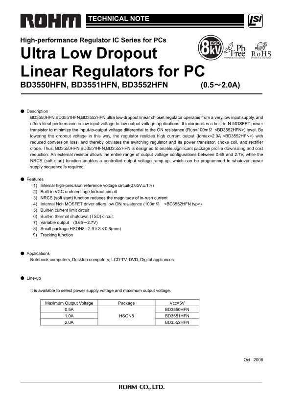
Ultra Low Dropout Linear Regulators for PC BD3550HFN, BD3551HFN, BD3552HFN (0.5~2.0A) ● Description BD3550HFN,BD3551HFN,BD3552HFN ultra low-dropout linear chipset regulator operates from a very low input supply, and offers ideal performance in low input voltage to low output voltage applications. It incorporates a built-in N-MOSFET power transistor to minimize the input-to-output voltage differential to the ON resistance (RON=100mΩ <BD3552HFN>) level. By lowering the dropout voltage in this way, the regulator realizes high current output (Iomax=2.0A <BD3552HFN>) with reduced conversion loss, and thereby obviates the switching regulator and its power transistor, choke coil, and rectifier diode. Thus, BD3550HFN,BD3551HFN,BD3552HFN is designed to enable significant package profile downsizing and cost reduction. An external resistor allows the entire range of output voltage configurations between 0.65 and 2.7V, while the NRCS (soft start) function enables a controlled output voltage ramp-up, which can be programmed to whatever power supply sequence is required. ● Features 1) Internal high-precision reference voltage circuit(0.65V±1%) 2) Built-in VCC undervoltage lockout circuit 3) NRCS (soft start) function reduces the magnitude of in-rush current 4) Internal Nch MOSFET driver offers low ON resistance (100mΩ <BD3552HFN typ>) 5) Built-in current limit circuit 6) Built-in thermal shutdown (TSD) circuit 7) Variable output (0.65~2.7V) 8) Small package HSON8 : 2.9×3×0.6(mm) 9) Tracking function

● Applications Notebook computers, Desktop computers, LCD-TV, DVD, Digital appliances

● Line-up

It is available to select power supply voltage and maximum output voltage.

Maximum Output Voltage Package Vcc=5V

0.5A BD3550HFN 1.0A BD3551HFN HSON8 2.0A BD3552HFN

Oct. 2008

Page Summary Contents For ROHM BD3550HFN Data Sheet

Page 1 TECHNICAL NOTE High-performance Regulator IC Series for PCs Ultra Low Dropout Linear Regulators for PC BD3550HFN, BD3551HFN, BD3552HFN (0.5~2.0A) ● Description BD3550HFN,BD3551HFN,BD3552HFN ultra low-...
Page 2 ●Absolute maximum ratings ◎BD3550HFN,BD3551HFN,BD3552HFN Limit Parameter Symbol Unit BD3550HFN BD3551HFN BD3552HFN Input Voltage 1 VCC +6.0 *1 V Input Voltage 2 VIN +6.0 *1 V Enable Input Voltage Ven ...
Page 3 ◎BD3550HFN,BD3551HFN,BD3552HFN ●Operating Voltage(Ta=25℃) Parameter Symbol Min. Max. Unit Input Voltage 1 VCC 4.3 5.5 V Input Voltage 2 VIN 0.95 VCC-1 *5 V Output Voltage Setting Range Vo VFB 2.7 V En...
Page 4 ●Reference Data(BD3550HFN) Vo Vo Vo 50m V/div 50m V/div 50m V/div Io Io Io 0.5A/div 0.5A/div 0.5A/div Io=0A→1A/μsec t(10μsec/div) Io=0A→1A/μsec t(10μsec/div) Io=0A→1A/μsec t(10μsec/div) Fig.1 Transien...
Page 5 ●Reference Data(BD3552HFN) Vo Vo Vo 50m V/div 50m V/div 50m V/div Io Io Io 2.0A/div 2.0A/div 2.0A/div Io=0A→1A/μsec t(10μsec/div) Io=0A→1A/μsec t(10μsec/div) Io=0A→1A/μsec t(10μsec/div) Fig.13 Transie...
Page 6 ●Reference Data(BD3551HFN) IC (m Ie (u IN (u VCC VCC Ven Ven VIN VIN Vo Vo 1.15 VIN→Ven→VCC Ven→VIN→VCC -10 Ta(℃) Fig.25 Input sequence Fig.26 Input sequence Fig.27 Ta-Vo (Io=0m A) (u IC (u Ta(℃) Ta(℃...
Page 7 ●Block Diagram 6M ax 2. ±0 .2 VCC Current Reference Limit Block CL UVLO Thermal FB Shutdown GNDNRCS ●Pin Layout PIN No. PIN name PIN Function 1 VCC Power supply pin 2 EN Enable input pin 3 GATE Gate p...
Page 8 ●Operation of Each Block ・AMP This is an error amp that compares the reference voltage (0.65V) with Vo to drive the output Nch FET (Ron=100m Ω:BD3552HFN). Frequency optimization helps to realize rapid...
Page 9 ●Timing Chart EN ON/OFF 0.65V(typ) Startup VCC ON/OFF Hysteresis UVLO 0.65V(typ) Startup Tracking sequence 1.8V Output 1.2V Output DC/DC 1.8V Vo Tracking sequence 1.2V 1.8V R1 FB Ratio-metric sequence
Page 10 ●Evaluation Board ■ BD3550HFN,BD3551HFN,BD3552HFN Evaluation Board Schematic GND_S VCC GND SW1 R8 GND U1 BD355XHFN EN NRCS (HSON8) GND C10 R1 GND GND FB C11 R4 GATE C13 R2 Vo_S VIN_S VIN R3 GND GND GN...
Page 11 ●Recommended Circuit Example GND VCC C1 EN R4 FB R2 C5 VOUT1(1.2V) C3 C2 VIN Recommended Component Programming Notes and Precautions Value R1/R2 3.9k/3.3k IC output voltage can be set with a configura...
Page 12 ●Heat Loss Thermal design should allow operation within the following conditions. Note that the temperatures listed are the allowed temperature limits, and thermal design should allow sufficient margi...
Page 13 ●Input-Output Equivalent Circuit Diagram NRCS 1kΩ VIN 1kΩ VFB 1kΩ EN VO2 50kΩ ●Reference landing pattern (Unit:mm) Lead pitch Lead pitch landing length landing pitch MIE ≧l2 b2 0.65 2.50 0.40 0.35 cen...
Page 14 ●Operation Notes 1. Absolute maximum ratings An excess in the absolute maximum ratings, such as supply voltage, temperature range of operating conditions, etc., can break down the devices, thus making...
Page 15 11. Regarding input pin of the IC This monolithic IC contains P+ isolation and P substrate layers between adjacent elements in order to keep them isolated. P-N junctions are formed at the intersection...
Page 16 ●Type Designations (Ordering Information) 6M ax 2. ±0 .2 Product Name Package Type TR Emboss tape reel opposite draw-out side: 1 pin ・BD355X ・HFN : HSON8 HSON8 &lt;Dimension&gt; &lt;Tape and Reel info...
Page 17 Appendix Notes No copying or reproduction of this document, in part or in whole, is permitted without the consent of ROHM CO.,LTD. The content specified herein is subject to change for improvement wit...

Manual Details

Brand ROHM
Pages 17
File Size 663.97 KB
Published June 18, 2026
1 views

Enter the captcha to get the download link:

captcha

Frequently Asked Questions

How is the output voltage configured if I need a specific range between 0.65V and 2.7V?

Use an external resistor, which allows for the entire range of output voltage configurations from 0.65V to 2.7V.

What benefit does the NRCS (soft start) function provide during power-up?

The soft start function enables a controlled output voltage ramp-up, reducing the magnitude of the in-rush current.

Is this regulator suitable for critical safety systems like aerospace or medical devices?

No. The product is not designed for use with equipment requiring an extremely high level of reliability, such as medical instruments or transportation equipment.

What is the maximum continuous output current available in the line-up?

The BD3552HFN offers a high current output of up to 2.0A.