ROHM BD3533HFN Data Sheet
Summary
The BD3533HFN is a specialized Regulator IC designed for high-precision memory signal termination in Dual Channel (DDR-II) applications. This manual provides developers with comprehensive technical specifications, detailing electrical characteristics, absolute maximum ratings, and operational limits necessary for reliable integration into electronic circuits. It is essential reading for system designers developing boards that require precise voltage regulation for advanced memory interface requirements.
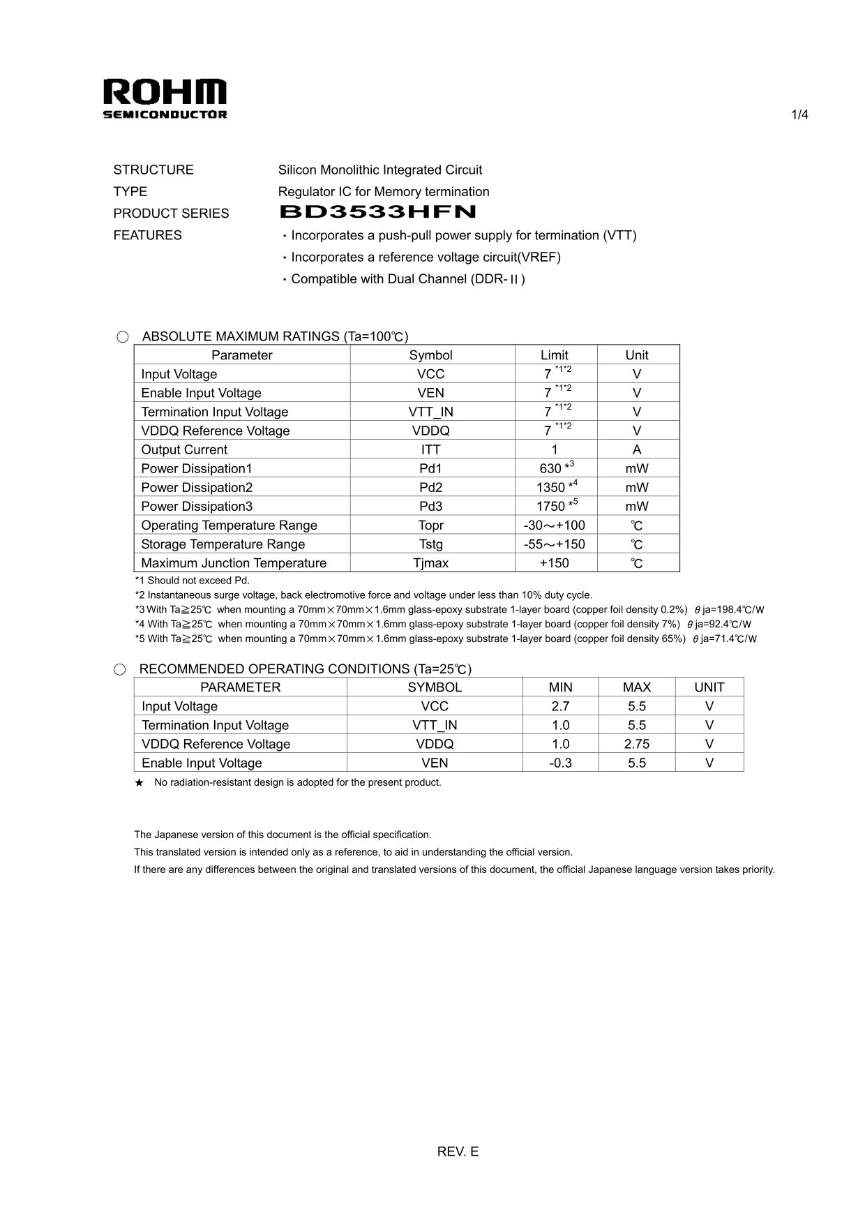
Page 1 Text Content
STRUCTURE Silicon Monolithic Integrated Circuit TYPE Regulator IC for Memory termination PRODUCT SERIES BD3533HFN FEATURES ・Incorporates a push-pull power supply for termination (VTT) ・Incorporates a reference voltage circuit(VREF) ・Compatible with Dual Channel (DDR-Ⅱ)
○ ABSOLUTE MAXIMUM RATINGS (Ta=100℃)
Parameter Symbol Limit Unit
Input Voltage VCC 7 *1*2 V Enable Input Voltage VEN 7 *1*2 V Termination Input Voltage VTT_IN 7 *1*2 V VDDQ Reference Voltage VDDQ 7 *1*2 V Output Current ITT 1 A Power Dissipation1 Pd1 630 *3 m W Power Dissipation2 Pd2 1350 *4 m W Power Dissipation3 Pd3 1750 *5 m W Operating Temperature Range Topr -30~+100 Storage Temperature Range Tstg -55~+150 Maximum Junction Temperature Tjmax +150 ℃ *1 Should not exceed Pd. *2 Instantaneous surge voltage, back electromotive force and voltage under less than 10% duty cycle. *3 With Ta≧25℃ when mounting a 70mm×70mm×1.6mm glass-epoxy substrate 1-layer board (copper foil density 0.2%) θja=198.4℃/W *4 With Ta≧25℃ when mounting a 70mm×70mm×1.6mm glass-epoxy substrate 1-layer board (copper foil density 7%) θja=92.4℃/W *5 With Ta≧25℃ when mounting a 70mm×70mm×1.6mm glass-epoxy substrate 1-layer board (copper foil density 65%) θja=71.4℃/W
○ RECOMMENDED OPERATING CONDITIONS (Ta=25℃)
PARAMETER SYMBOL MIN MAX UNIT
Input Voltage VCC 2.7 5.5 V Termination Input Voltage VTT_IN 1.0 5.5 V VDDQ Reference Voltage VDDQ 1.0 2.75 V Enable Input Voltage VEN -0.3 5.5 V ★ No radiation-resistant design is adopted for the present product.
The Japanese version of this document is the official specification. This translated version is intended only as a reference, to aid in understanding the official version. If there are any differences between the original and translated versions of this document, the official Japanese language version takes priority.
REV. E
Page Summary Contents For ROHM BD3533HFN Data Sheet
Manual Details
| Brand | ROHM |
|---|---|
| Pages | 5 |
| File Size | 127.56 KB |
| Published | July 12, 2026 |
Enter the captcha to get the download link:

Frequently Asked Questions
What type of memory architecture is this regulator IC designed for?
It is compatible with Dual Channel (DDR-Ⅱ) memory.
What are the normal operating voltage ranges for VCC and TTT_IN?
The recommended range for Input Voltage (VCC) is 2.7 to 5.5 V, and for Termination Input Voltage (VTTS_IN) is 1.0 to 5.5 V.
Can this product be used in specialized high-reliability or radiation-tolerant systems?
No. The device is not designed to be radiation tolerant, and the manufacturer strongly warns against using it in safety-critical equipment.
What is the Standby Current Draw (IST) when the Enable Pin (VEN) is set to 0V?
The typical standby current (IST) is rated between -0.5 mA and 1.0 mA.