# A B C D E F G H I J K L M N O P Q R S T U V W X Y Z

ROHM BD2051AFJ BD2041AFJ BD6519FJ Data Sheet

Summary

This single-channel high side switch IC is optimized for reliable power management in USB applications, efficiently controlling power over a 2.7V to 5.5V range. The device features built-in safety mechanisms including Over Current Protection (OCP), Thermal Shutdown (TSD), and Under Voltage Lockout (UVLO). This comprehensive manual provides engineers with critical data on specifications, operational curves, and pin configurations required for designing durable power systems. It is ideal for use in consumer electronics such as USB hubs, PC peripherals, and car accessories that demand low-resistance switching performance.
📄 Preview PAGE OF 25

Page 1 Text Content

Datasheet

1 Channel High Side Switch ICs

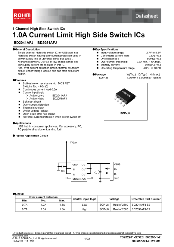
1.0A Current Limit High Side Switch ICs BD2041AFJ BD2051AFJ ●General Description ●Key Specifications Single channel high side switch IC for USB port is a Input voltage range: 2.7V to 5.5V high side switch having over current protection used in Continuous current load: 0.5A(Typ.) power supply line of universal serial bus (USB). ON resistance : 80mΩ(Typ.) N-channel power MOSFET of low on resistance and Over current threshold: 0.7A min., 1.6A max. low supply current are realized in this IC. Standby current: 0.01μA (Typ.) And, over current detection circuit, thermal shutdown Operating temperature range: -40℃ to +85℃ circuit, under voltage lockout and soft start circuit are built in. ●Package W(Typ.) D(Typ.) H (Max.)

SOP-J8 4.90mm x 6.00mm x 1.65mm

●Features Built-in low on resistance Nch MOS FET Switch.( Typ = 80mΩ) Continuous current load 0.5A Control input logic

Active-Low : BD2041AFJ Active-High: BD2051AFJ Soft start circuit Over current detection Thermal shutdown Under voltage lockout

Open drain error flag output SOP-J8

Reverse-current protection when power switch off

●Applications USB hub in consumer appliances, Car accessory, PC, PC peripheral equipment, and so forth

●Typical Application Circuit

5V(typ.)

GND VBUS OUT

OUT IN D+

IN OUT D-

EN(/EN) /OC GND

●Lineup

Over current detection

Control input logic Package Orderable Part Number Min. Typ. Max.

0.7A 1.0A 1.6A Low SOP-J8 Reel of 2500 BD2041AFJ-E2 0.7A 1.0A 1.6A High SOP-J8 Reel of 2500 BD2051AFJ-E2

○Product structure:Silicon monolithic integrated circuit ○This product is not designed protection against radioactive rays www.rohm.com © 2013 ROHM Co., Ltd. All rights reserved. TSZ02201-0E3E0H300290-1-2

TSZ22111・14・001 08.Mar.2013 Rev.001

Page Summary Contents For ROHM BD2051AFJ BD2041AFJ BD6519FJ Data Sheet

Page 1 Datasheet 1 Channel High Side Switch ICs 1.0A Current Limit High Side Switch ICs BD2041AFJ BD2051AFJ ●General Description ●Key Specifications Single channel high side switch IC for USB port is a Input...
Page 2 Datasheet BD2041AFJ BD2051AFJ ●Block Diagram GND OUT IN Charge OCD UVLO OUT IN Gate logic OUT TSD /OC EN(/EN) ●Pin Configurations BD2041AFJ BD2051AFJ TOP VIEW TOP VIEW OUT GND OUT IN OUT IN OUT IN OUT...
Page 3 Datasheet BD2041AFJ BD2051AFJ ●Absolute Maximum Ratings Parameter Symbol Limits Unit Supply voltage VIN -0.3 to 6.0 V Enable voltage VEN, V/EN -0.3 to 6.0 V /OC voltage V/OC -0.3 to 6.0 V /OC current ...
Page 4 Datasheet BD2041AFJ BD2051AFJ ●Electrical Characteristics-Continued ◎BD2051AFJ (Unless otherwise specified, VIN = 5.0V, Ta = 25°C) Limits Parameter Symbol Unit Condition Min. Typ. Max. Operating Curre...
Page 5 Datasheet BD2041AFJ BD2051AFJ ●Measurement Circuit GND OUT GND OUT IN OUT IN OUT IN OUT IN OUT RL CL EN(/EN) /OC EN(/EN) /OC VEN(V/EN) VEN(V/EN) A. Operating current B. EN, /EN input voltage, Output r...
Page 6 Datasheet BD2041AFJ BD2051AFJ ●Typical Performance Curves IS TB [μ ID [μ Ta=25°C VIN=5.0V IS TB [μ ID [μ -50 SUPPLY VOLTAGE : VIN[V] AMBIENT TEMPERATURE : Ta[℃] Figure 4. Operating current Figure 5. O...
Page 7 Datasheet BD2041AFJ BD2051AFJ /O TP LO LT LE IN LT V/ [V VE , V /E ] 0 ●Typical Performance Curves – Continued 2.0 2.0 Ta=25°C VIN=5.0V Low to High Low to High High to Low High to Low /O TP LO LT LE I...
Page 8 Datasheet BD2041AFJ BD2051AFJ IS TA IR IT ●Typical Performance Curves – Continued Ta=25°C VIN=5.0V IR IT IS TA SC [A [m -50 SUPPLY VOLTAGE : VIN[V] AMBIENT TEMPERATURE : Ta[℃] Figure 12. ON resistance...
Page 9 Datasheet BD2041AFJ BD2051AFJ IS IM TU IM ●Typical Performance Curves – Continued TO [m s] TO [m s] Ta=25°C VIN=5.0V TU IM IS IM TO [m s] TO [m s] SUPPLY VOLTAGE : VIN[V] AMBIENT TEMPERATURE : Ta[℃] F...
Page 10 Datasheet BD2041AFJ BD2051AFJ FF IM FA LL IM ●Typical Performance Curves – Continued TO FF [μ s] FF [μ s] Ta=25°C VIN=5.0V FF IM FA LL IM TO FF [μ s] TO FF [µ s] SUPPLY VOLTAGE : VIN[V] AMBIENT TEMPER...
Page 11 Datasheet BD2041AFJ BD2051AFJ LO LD LT ●Typical Performance Curves – Continued LO H, LO L[V VUVLOH VUVLOL LO TE IS LT AG :V AMBIENT TEMPERATURE : Ta[℃] AMBIENT TEMPERATURE: Ta[℃] AM BIENT TEM PERATURE...
Page 12 Datasheet BD2041AFJ BD2051AFJ ●Typical Wave Forms V/EN V/EN (5V/div.) (5V/div.) (5V/div.) (5V/div.) (5V/div.) (5V/div.) VIN=5V RL=10Ω IOUT CL=100μF (0.5A/div.) VIN=5V (0.5A/div.) RL=10Ω CL=100μF TIME(...
Page 13 Datasheet BD2041AFJ BD2051AFJ ●Typical Wave Forms – Continued V/OC V/EN (5V/div.) (5V/div.) VOUT V/OC (5V/div.) (5V/div.) VOUT (5V/div.) IOUT IOUT VIN=5V (0.5A/div.) VIN=5V (0.5A/div.) CL=100μF TIME(2...
Page 14 Datasheet BD2041AFJ BD2051AFJ ●Typical Wave Forms – Continued VIN VIN (5V/div.) (5V/div.) (5V/div.) (5V/div.) (0.5A/div.) (0.5A/div.) (5V/div.) (5V/div.) RL=10Ω RL=10Ω CL=147μF CL=147μF TIME (10ms/div...
Page 15 Datasheet BD2041AFJ BD2051AFJ ●Typical Application Circuit 5V(typ.) VBUS IN Regulator D- GND GND OUT VBUS 10k to 100kΩ OUTIN D+ Controller CL IN OUT EN(/EN) /OC GND ●Application Information When exces...
Page 16 Datasheet BD2041AFJ BD2051AFJ 3. Over current detection (OCD) The over current detection circuit limits current (ISC) and outputs error flag (/OC) when current flowing in each switch MOSFET exceeds a ...
Page 17 Datasheet BD2041AFJ BD2051AFJ ●Power Dissipation (SOP-J8) PO ER IS SI PA TI : P d[ AMBIENT TEMPERATURE: Ta [℃] Figure 38. Power dissipation curve (Pd-Ta Curve) ●I/O Equivalence Circuit Symbol Pin No E...
Page 18 Datasheet BD2041AFJ BD2051AFJ ●Operational Notes (1) Absolute Maximum Ratings An excess in the absolute maximum ratings, such as supply voltage, temperature range of operating conditions, etc., can br...
Page 19 Datasheet BD2041AFJ BD2051AFJ (10) Ground wiring pattern If small-signal GND and large-current GND are provided, It will be recommended to separate the large-current GND pattern from the small-signal ...
Page 20 Datasheet BD2041AFJ BD2051AFJ ●Ordering Information Part Number Package Packaging and forming specification FJ: SOP-J8 E2: Embossed tape and reel Part Number Package Packaging and forming specificatio...
Page 21 Datasheet BD2041AFJ BD2051AFJ ●Physical Dimension, Tape and Reel Information Package Name SOP-J8 <Tape and Reel information> Embossed carrier tape Tape Quantity 2500pcs Direction The direction i...
Page 22 Datasheet BD2041AFJ BD2051AFJ ●Revision History Date Revision Changes 08.Mar.2013 001 New Release www.rohm.com TSZ02201-0E3E0H300290-1-2 © 2013 ROHM Co., Ltd. All rights reserved. TSZ22111・15・001 08.M...
Page 23 Datasheet Notice ●General Precaution 1) Before you use our Products, you are requested to carefully read this document and fully understand its contents. ROHM shall not be in any way responsible or li...
Page 24 Datasheet ●Precaution for Mounting / Circuit board design 1) When a highly active halogenous (chlorine, bromine, etc.) flux is used, the residue of flux may negatively affect product performance and r...
Page 25 Datasheet ●Other Precaution 1) The information contained in this document is provided on an “as is” basis and ROHM does not warrant that all information contained in this document is accurate and/or e...

Manual Details

Brand ROHM
Pages 25
File Size 676.21 KB
Published June 15, 2026
2 views

Enter the captcha to get the download link:

captcha

Frequently Asked Questions

What is the operational voltage range for this high side switch IC?

The recommended operating voltage (VIN) is between 2.7V and 5.5V.

Which model uses Active-Low logic for control input?

The BD2041AFJ requires an Active-Low signal to activate the power switch.

What protective features are included in the circuit design?

It is built with over current detection, thermal shutdown, under voltage lockout (UVLO), and a soft start circuit.