Panasonic MN31121SA User Guide
Summary
This comprehensive guide details the MN31121SA, a specialized 2D interline CCD image sensor vertical driver IC. This miniature component streamlines camera development by integrating complex 2-value and 3-value output drivers, along with level shifter circuits on a single chip. The manual provides detailed specifications, operational parameters, pinouts, and comprehensive application notes. It is essential reading for engineers designing advanced video cameras, surveillance systems, and digital CCD image sensor platforms requiring maximum efficiency and reduced component count.
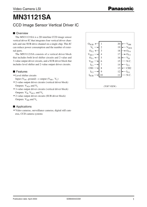
Page 1 Text Content
Video Camera LSI
MN31121SA CCD Image Sensor Vertical Driver IC Overview The MN31121SA is a 2D interline CCD image sensor vertical driver IC that integrates four vertical driver chan-
nels and one SUB drive channel on a single chip. This IC OSUB VHH can reduce power consumption and the number of exter- VL VM24
nal parts. OV2 OV4 The MN31121SA consists of a vertical driver block VM13 OV3 that includes both level shifter circuits and 2-value and OV1 VH 3-value output driver circuits, and a SUB driver block that VDC N.C. includes level shifter and 2-value output driver circuits. IV1 IV3
CH1 CH2 Features IV2 IV4 Level shifter circuits ISUB N.C.
Input (VDC, ground) → output (VHH , VL) 2-value output driver circuits (vertical driver block) Outputs: VM24 and VL (TOP VIEW) 3-value output driver circuits (vertical driver block) Outputs: VH, VM13, and VL 2-value output driver circuits (SUB driver block) Outputs: VHH and VL
Applications Video cameras, surveillance cameras, digital still cam- eras, CCD camera systems
Publication date: April 2003 SDB00054CEM
Page Summary Contents For Panasonic MN31121SA User Guide
Manual Details
| Brand | Panasonic |
|---|---|
| Pages | 11 |
| File Size | 173.27 KB |
| Published | June 18, 2026 |
Enter the captcha to get the download link:

Frequently Asked Questions
What applications is the MN31121SA designed for?
It is primarily intended for video cameras, surveillance cameras, digital still cameras, and general CCD camera systems.
Can this IC reduce component count or power consumption?
Yes, it integrates multiple channels on a single chip, which can reduce both power consumption and the number of external parts needed.
What is the operating temperature range?
The device operates at temperatures between -10°C to +70°C.
Are there specific requirements for using this IC in special applications?
For critical applications (e.g., aerospace or medical devices), users must consult sales staff regarding exceptional quality and reliability needs.