Panasonic 2SK3193 User Guide
Summary
This technical document provides comprehensive specifications for the 2SK3193 Silicon N-channel power MOSFET, a high-speed component known for low ON resistance and avalanche capability. Ideal for professional engineers and system designers building standard electronic equipment—such as communication devices or industrial appliances—this manual details electrical characteristics, absolute ratings, switching times, and optimal operating guidelines to ensure reliable power management applications.
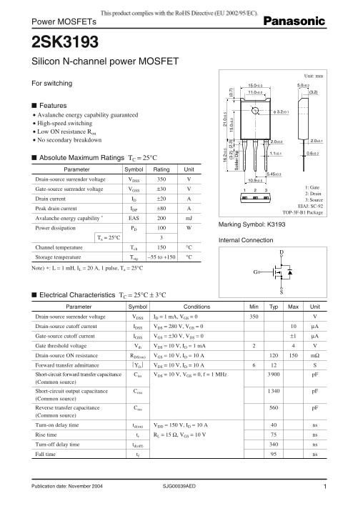
Page 1 Text Content
This product complies with the Ro HS Directive (EU 2002/95/EC).
Power MOSFETs
2SK3193 Silicon N-channel power MOSFET
Unit: mm
For switching 15.0±0.3 5.0±0.2
Features
Avalanche energy capability guaranteed High-speed switching Low ON resistance Ron No secondary breakdown 2.0±0.2 2.0±0.1
Absolute Maximum Ratings TC = 25°C Parameter Symbol Rating Unit
Drain-source surrender voltage VDSS 10.9±0.5
1: Gate
Gate-source surrender voltage VGSS ±30
2: Drain
Drain current ID ±20 3: Source
EIAJ: SC-92
Peak drain current IDP ±80
TOP-3F-B1 Package
Avalanche energy capability * EAS m J
Marking Symbol: K3193 .2 ±0 .5 .0 ±0 .5
Power dissipation PD
ol de ip
Ta = 25°C
Internal Connection
Channel temperature Tch °C Storage temperature Tstg −55 to +150 °C Note) L = 1 m H, IL = 20 A, 1 pulse, Ta = 25°C
Electrical Characteristics TC = 25°C ± 3°C Parameter Symbol Conditions Min Typ Max Unit Drain-source surrender voltage VDSS ID = 1 m A, VGS = 0 Drain-source cutoff current IDSS VDS = 280 V, VGS = 0 µA Gate-source cutoff current IGSS VGS = ±30 V, VDS = 0 ±1 µA Gate threshold voltage Vth VDS = 10 V, ID = 1 m A Drain-source ON resistance RDS(on) VGS = 10 V, ID = 10 A mΩ Forward transfer admittance Yfs VDS = 10 V, ID = 10 A Short-circuit forward transfer capacitance Ciss VDS = 10 V, VGS = 0, f = 1 MHz 3 900 p F (Common source) Short-circuit output capacitance Coss 1 340 p F (Common source) Reverse transfer capacitance Crss p F (Common source) Turn-on delay time td(on) VDD = 150 V, ID = 10 A ns Rise time tr RL = 15 Ω, VGS = 10 V ns Turn-off delay time td(off) ns Fall time tf ns
SJG00039AED 1Publication date: November 2004
Page Summary Contents For Panasonic 2SK3193 User Guide
Manual Details
| Brand | Panasonic |
|---|---|
| Pages | 3 |
| File Size | 101.13 KB |
| Published | June 20, 2026 |
Enter the captcha to get the download link:

Frequently Asked Questions
What regulations must this product adhere to?
The product complies with the RoHS Directive (EU 2002/95/EC).
What is the maximum drain current capability?
The absolute maximum rating for the drain current (Id) is ±20 A. The peak drain current (I DP) is ±80 A.
How should I calculate safe power dissipation?
Safe operation area P allows different power dissipations based on ambient temperature and drain-source voltage thresholds, such as 3 W at typical operating conditions without a heat sink.
What kind of applications are standard or recommended for this device?
It is intended for standard applications like office equipment, communications equipment, measuring instruments, and household appliances.