ON NCV8501 Series Micropower 150 mA LDO Linear Regulators Data Manual (1) Specification Sheet
Summary
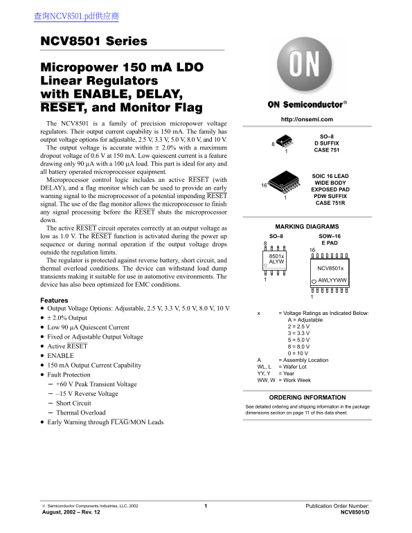
The NCV8501 series is a high-reliability micropower LDO linear voltage regulator designed for critical microprocessor applications. Offering adjustable or fixed output options and low quiescent current (90 μA), this regulator ensures stable power for battery-operated devices, even in demanding automotive environments. Key features include active RESET monitoring and an early warning FLAG signal for enhanced system control. This technical resource provides detailed electrical characteristics, package connections, and maximum ratings required to optimally integrate the device into your next design.
Page 1 Text Content
查询NCV8501.pdf供应商
NCV8501 Series
Micropower 150 m A LDO Linear Regulators with ENABLE, DELAY, RESET, and Monitor Flag
http://onsemi.com
The NCV8501 is a family of precision micropower voltage regulators. Their output current capability is 150 m A. The family has
output voltage options for adjustable, 2.5 V, 3.3 V, 5.0 V, 8.0 V, and 10 V.
D SUFFIX
The output voltage is accurate within ± 2.0% with a maximum
CASE 7511
dropout voltage of 0.6 V at 150 m A. Low quiescent current is a feature drawing only 90 µA with a 100 µA load. This part is ideal for any and all battery operated microprocessor equipment.
SOIC 16 LEAD
Microprocessor control logic includes an active RESET (with
WIDE BODY
DELAY), and a flag monitor which can be used to provide an early
EXPOSED PAD
warning signal to the microprocessor of a potential impending RESET PDW SUFFIX
signal. The use of the flag monitor allows the microprocessor to finish CASE 751R
any signal processing before the RESET shuts the microprocessor down.
The active RESET circuit operates correctly at an output voltage as MARKING DIAGRAMS low as 1.0 V. The RESET function is activated during the power up SO–8 SOW–16
sequence or during normal operation if the output voltage drops E PAD
outside the regulation limits.
The regulator is protected against reverse battery, short circuit, and ALYW
thermal overload conditions. The device can withstand load dump NCV8501x
transients making it suitable for use in automotive environments. The
AWLYYWW
device has also been optimized for EMC conditions.
Features Output Voltage Options: Adjustable, 2.5 V, 3.3 V, 5.0 V, 8.0 V, 10 V
= Voltage Ratings as Indicated Below:
± 2.0% Output
A = Adjustable Low 90 µA Quiescent Current 2 = 2.5 V 3 = 3.3 V
Fixed or Adjustable Output Voltage
Active RESET 8 = 8.0 V
ENABLE
= Assembly Location
150 m A Output Current Capability WL, L = Wafer Lot
Fault Protection YY, Y = Year WW, W = Work Week
+60 V Peak Transient Voltage –15 V Reverse Voltage
ORDERING INFORMATION
Short Circuit
See detailed ordering and shipping information in the package Thermal Overload dimensions section on page 11 of this data sheet.
Early Warning through FLAG/MON Leads
Semiconductor Components Industries, LLC, 2002 Publication Order Number: August, 2002 – Rev. 12 NCV8501/D
Page Summary Contents For ON NCV8501 Series Micropower 150 mA LDO Linear Regulators Data Manual (1) Specification Sheet
Manual Details
| Brand | Linear |
|---|---|
| Pages | 16 |
| File Size | 111.93 KB |
| Published | June 16, 2026 |
Enter the captcha to get the download link:

Frequently Asked Questions
What is the maximum output current for this regulator?
The NCV8501 family has an output current capability of 150 mA.
Does the device offer protection against power surges or fluctuations?
Yes, it provides protection against reverse battery, short circuits, thermal overload, and load dump transients.
How does the FLAG/RESET monitor assist the system during power changes?
It allows the microprocessor to finish signal processing by providing an early warning before a potential full RESET shutdown.
Is this regulator suitable for specific harsh environments like vehicles?
Yes, it can withstand load dump transients and has been optimized for EMC conditions, making it suitable for automotive environments.