National Semiconductor MM54C48 MM74C48 BCD-to-7 Segment Decoder
Summary
The MM54C48/MM74C48 is a high-performance CMOS integrated circuit designed to convert Binary Coded Decimal (BCD) data into signals suitable for driving 7-segment displays. This comprehensive technical manual provides circuit designers and engineers with detailed electrical characteristics, absolute maximum ratings, and timing specifications—including ripple blanking and lamp test options. Ideal for advanced digital display systems requiring reliable, low-power decoding across varied operating voltages (3.0V to 15V).
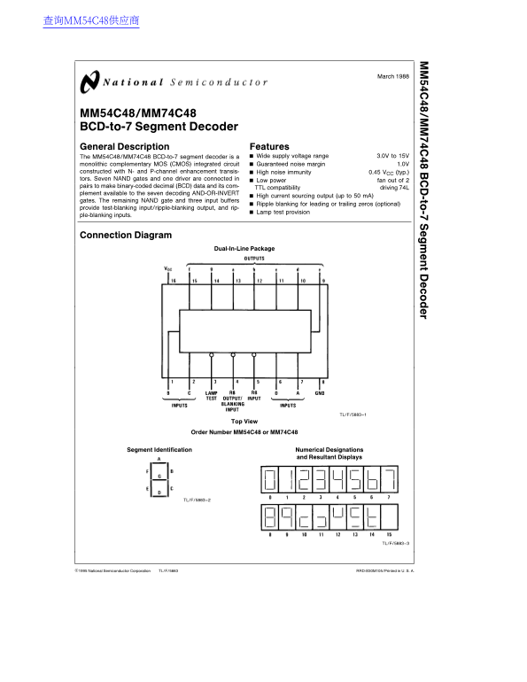
Page 1 Text Content
查询MM54C48供应商
March
-to -7
MM54C48/MM74C48 BCD-to-7 Segment Decoder General Description Features
The MM54C48/MM74C48 BCD-to-7 segment decoder is Wide supply voltage range 3.0V to 15V
monolithic complementary MOS (CMOS) integrated circuit Guaranteed noise margin 1.0V constructed with N- and P-channel enhancement transis- High noise immunity 0.45 VCC (typ.) tors. Seven NAND gates and one driver are connected in Low power fan out of pairs to make binary-coded decimal (BCD) data and its com- TTL compatibility driving 74L plement available to the seven decoding AND-OR-INVERT
High current sourcing output (up to m A)
gates. The remaining NAND gate and three input buffers
Ripple blanking for leading or trailing zeros (optional)
provide test-blanking input/ripple-blanking output, and rip-
Lamp test provision
ple-blanking inputs.
Connection Diagram
Dual-In-Line Package
TL/F/5883–1
Order Number MM54C48 or MM74C48
Segment Identification Numerical Designations and Resultant Displays
TL/F/5883–2
TL/F/5883–3
C1995 National Semiconductor Corporation TL/F/5883 RRD-B30M105/Printed in U. S. A.
Page Summary Contents For National Semiconductor MM54C48 MM74C48 BCD-to-7 Segment Decoder
Manual Details
| Brand | National |
|---|---|
| Pages | 6 |
| File Size | 131.10 KB |
| Published | June 15, 2026 |
Enter the captcha to get the download link:

Frequently Asked Questions
What does the MM54C48/MM74C48 decoder convert?
This circuit converts binary-coded decimal (BCD) data to a standard 7-segment display signal.
What is the recommended operating voltage range?
The device can operate across a wide range of power supply voltages, from 3.0V to 15V.
How much electrical current can the output drive?
The chip has high current sourcing outputs, up to 50 mA.
What are the temperature limitations for use?
The operating temperature range varies by specific component model (e.g., -40°C to +85°C).