National Semiconductor MM54C42 MM74C42 BCD-to-Decimal Decoder Data Sheet Owner's Manual
Summary
This advanced CMOS one-of-ten decoder efficiently converts a four-bit Binary Coded Decimal (BCD) input into a unique active digital signal. Suitable for professional engineers designing robust electronic systems, this integrated circuit provides predictable decoding logic in applications ranging from industrial controls and automotive alarm systems to computing devices. The accompanying manual provides comprehensive technical specifications, electrical characteristics, and operational guidelines necessary for reliable circuit implementation.
Page 1 Text Content
查询MM54C42供应商
March
-to -D im
MM54C42/MM74C42 BCD-to-Decimal Decoder General Description
The MM54C42/MM74C42 one-of-ten decoder is mono- High noise immunity 0.45 VCC (typ.)
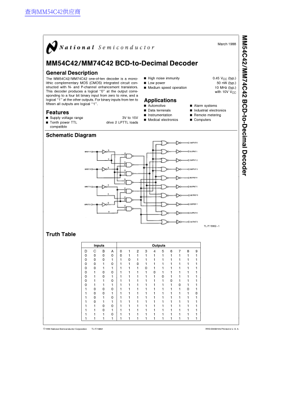
lithic complementary MOS (CMOS) integrated circuit con- Low power n W (typ.) structed with N- and P-channel enhancement transistors. Medium speed operation MHz (typ.) This decoder produces logical ‘‘0’’ at the output corre- with 10V VCC sponding to four bit binary input from zero to nine, and logical ‘‘1’’ at the other outputs. For binary inputs from ten to Applications fifteen all outputs are logical ‘‘1’’.
Automotive Alarm systems Data terminals Industrial electronics
Features
Instrumentation Remote metering
Supply voltage range 3V to 15V
Medical electronics Computers
Tenth power TTL drive LPTTL loads compatible
Schematic Diagram
TL/F/5882–1
Truth Table
Inputs Outputs
C1995 National Semiconductor Corporation TL/F/5882 RRD-B30M105/Printed in U. S. A.
Page Summary Contents For National Semiconductor MM54C42 MM74C42 BCD-to-Decimal Decoder Data Sheet Owner's Manual
Manual Details
| Brand | National |
|---|---|
| Pages | 4 |
| File Size | 107.52 KB |
| Published | June 18, 2026 |
Enter the captcha to get the download link:

Frequently Asked Questions
What is the primary function of the MM54C42 decoder?
It acts as a one-of-ten decoder, converting a four-bit binary input into specific logical '0' or '1' outputs.
What is the permissible operating voltage range for this device?
The supply voltage range is within 3V to 15V
Are there any usage limitations regarding safety-critical applications?
No, its use in life support devices or critical systems requires written approval from National Semiconductor Corporation.