National Semiconductor CLC5612 Dual, High Output, Programmable Gain Buffer User Guide and Data Sheet
Summary
This high-speed dual programmable gain buffer is an ideal solution for demanding professional and consumer video applications. It features multiple robust output stages—including coaxial cable, twisted pair, and transformer/coil drivers—delivering a high 130mA output current while maintaining low power consumption. The associated manual provides comprehensive technical details on the unit's performance, including frequency bandwidth (up to 90MHz), settling times, distortion figures, and stability across various capacitive loads. Perfect for portable, battery-powered systems or any application requiring superior high-speed signal integrity.
Page 1 Text Content
查询CLC5612供应商
June 1999
al,H ig tp t,P ro ram ab le G ain ffer
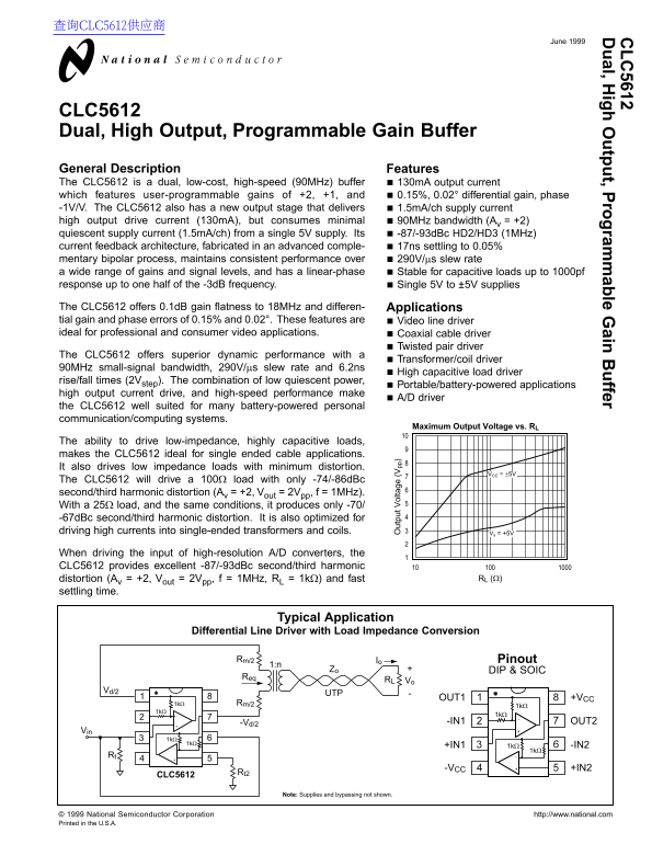
CLC5612 Dual, High Output, Programmable Gain Buffer General Description Features The CLC5612 is a dual, low-cost, high-speed (90MHz) buffer 130m A output current which features user-programmable gains of +2, +1, and 0.15%, 0.02° differential gain, phase -1V/V. The CLC5612 also has a new output stage that delivers 1.5m A/ch supply current high output drive current (130m A), but consumes minimal 90MHz bandwidth (Av = +2) quiescent supply current (1.5m A/ch) from a single 5V supply. Its -87/-93d Bc HD2/HD3 (1MHz) current feedback architecture, fabricated in an advanced comple- 17ns settling to 0.05% mentary bipolar process, maintains consistent performance over 290V/µs slew rate a wide range of gains and signal levels, and has a linear-phase Stable for capacitive loads up to 1000pf response up to one half of the -3d B frequency. Single 5V to ±5V supplies The CLC5612 offers 0.1d B gain flatness to 18MHz and differen- Applications tial gain and phase errors of 0.15% and 0.02°. These features are Video line driver ideal for professional and consumer video applications. Coaxial cable driver
Twisted pair driver
The CLC5612 offers superior dynamic performance with a
Transformer/coil driver
90MHz small-signal bandwidth, 290V/µs slew rate and 6.2ns
High capacitive load driver
rise/fall times (2Vstep). The combination of low quiescent power,
Portable/battery-powered applications
high output current drive, and high-speed performance make
ut pu t V ol ta ge pp A/D driver
the CLC5612 well suited for many battery-powered personal communication/computing systems.
Maximum Output Voltage vs. RL
The ability to drive low-impedance, highly capacitive loads, makes the CLC5612 ideal for single ended cable applications. It also drives low impedance loads with minimum distortion.
VCC = ±5V
The CLC5612 will drive a 100Ω load with only -74/-86d Bc second/third harmonic distortion (Av = +2, Vout = 2Vpp, f = 1MHz). With a 25Ω load, and the same conditions, it produces only -70/ -67d Bc second/third harmonic distortion. It is also optimized for driving high currents into single-ended transformers and coils. Vs = +5V
When driving the input of high-resolution A/D converters, the CLC5612 provides excellent -87/-93d Bc second/third harmonic
distortion (Av = +2, Vout = 2Vpp, f = 1MHz, RL = 1kΩ) and fast RL (Ω)
settling time.
Typical Application
Differential Line Driver with Load Impedance Conversion
Rm/2 Io Pinout 1:n
Zo DIP & SOIC
RL Vo
OUT1 +VCC
1kΩ Rm/2
-Vd/2 -IN1 OUT2
+IN1 1kΩ -IN2
-VCC +IN2
CLC5612
Note: Supplies and bypassing not shown.
1999 National Semiconductor Corporation http://www.national.com Printed in the U.S.A.
Page Summary Contents For National Semiconductor CLC5612 Dual, High Output, Programmable Gain Buffer User Guide and Data Sheet
Manual Details
| Brand | National |
|---|---|
| Pages | 12 |
| File Size | 202.62 KB |
| Published | June 16, 2026 |
Enter the captcha to get the download link:

Frequently Asked Questions
What high-speed applications is the CLC5612 suitable for?
It is ideal for professional and consumer video applications, such as differential and coaxial cable driving.
How much output current can this buffer provide?
It has a high output drive current of 130mA per channel.
Does the CLC5612 provide adjustable gain settings?
Yes, it features user-programmable gains of +2, +1, and nominal (n) settings.
What is the input capacitance specification?
The non-inverting input capacitance is specified as 2.2 to 3.3 pF.