National Semiconductor CLC111 Ultra High Slew Rate, Closed Loop Buffer Data Sheet
Summary
The CLC111 is an ultra-high slew rate, closed-loop buffer engineered for reliable signal processing in demanding applications like video switching and high-frequency filtering. It features superior performance metrics, including an 800MHz bandwidth and a massive 3500V/µs slew rate, making it ideal for single-supply, power-sensitive circuits. This manual provides comprehensive technical specifications, electrical characteristics, and application guidance, helping engineers select the correct version for industrial, military, or high-speed consumer electronics designs.
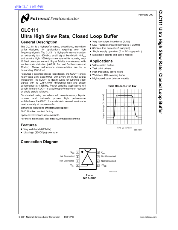
Page 1 Text Content
查询CLC111供应商
February
LC ltra igh lew ate,C losed Loop uffer
CLC111 Ultra High Slew Rate, Closed Loop Buffer
Very low output impedance (1.4Ω)
General Description
Low (−62d Bc) 2nd/3rd harmonics 20MHz
The CLC111 is high performance, closed loop, monolithic
60m A output current (±5 supplies)
buffer designed for applications requiring very high
Single supply operation (0 to 3V supply min.)
frequency signals. The CLC111’s high performance includes
Evaluation boards and Spice models
an extremely fast 800MHz small signal bandwidth (0.5pp) and an ultra high (3500V/µs) slew rate while requiring only 10.5m A quiescent current. Signal fidelity is maintained with Applications low harmonic distortion (−62d Bc 2nd and 3rd harmonics at
Video switch buffers
20MHz). These performance characteristics are for
Test point drivers
demanding 100Ω load.
High frequency active filters
Featuring patented closed loop design, the CLC111 offers
Wideband DC clamping buffer
nearly ideal unity gain (0.996) with very low (1.4Ω) output
High-speed peak detector circuits
impedance. The CLC111 is ideally suited for buffering video signals with its 0.15%/0.04˚ differential gain and phase performance at 4.43MHz. Power sensitive applications will Pulse Response for ±5V benefit from the CLC111’s excellent performance on reduced or single supply voltages. Constructed using an advanced, complementary bipolar process and National’s proven high performance architectures, the CLC111 is available in several versions to meet variety of requirements. Enhanced Solutions (Military/Aerospace) SMD Number: contact factory Space level versions also available. For more information, visit http://www.national.com/mil
Features Very wideband (800MHz) DS012720-1 Ultra high (3500V/µs) slew rate
Connection Diagram
DS012720-2
Pinout DIP SOIC
National Semiconductor Corporation DS012720 www.national.com
Page Summary Contents For National Semiconductor CLC111 Ultra High Slew Rate, Closed Loop Buffer Data Sheet
Manual Details
| Brand | National |
|---|---|
| Pages | 10 |
| File Size | 254.37 KB |
| Published | June 06, 2026 |
Enter the captcha to get the download link:

Frequently Asked Questions
What is the maximum small-signal bandwidth?
The Small Signal Bandwidth (SSBW) can reach 800 MHz.
Does it support single supply operation?
Yes, the CLC111 supports single supply operation from 0 to 3V minimum.
What is the output current capability?
It features a 60mA output current (with ±5 supplies).
Which packages are available?
It is available in SOIC, Plastic DIP, and other versions (e.g., Military/Aerospace).