Motorola MC10E256 MC100E256 Data Sheet (1) User Manual
Summary
This advanced semiconductor chip integrates powerful MUX-Latch functionality with differential outputs, offering precise control through select and enable signals. The comprehensive technical manual provides electronics engineers and hardware designers with all necessary details for implementation. Content includes detailed operational tables, pin configurations, crucial AC/DC electrical characteristics (such as timing delays), and mechanical specifications, ensuring reliable integration into professional digital logic circuits.
Page 1 Text Content
SEMICONDUCTOR TECHNICAL DATA
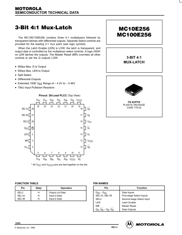
The MC10E/100E256 contains three 4:1 multiplexers followed by transparent latches with differential outputs. Separate Select controls are provided for the leading 2:1 mux pairs (see logic symbol). When the Latch Enable (LEN) is LOW, the latch is transparent, and output data is controlled by the multiplexer select controls. A logic HIGH on LEN latches the outputs. The Master Reset (MR) overrides all other
controls to set the Q outputs LOW. 3-BIT 4:1 MUX-LATCH
950ps Max. D to Output 850ps Max. LEN to Output Split Select Differential Outputs Extended 100E VEE Range of – 4.2V to – 5.46V 75kΩ Input Pulldown Resistors
Pinout: 28-Lead PLCC (Top View) D1b D1a D2d D2c D2b D2a VCCO
FN SUFFIX PLASTIC PACKAGE CASE 776-02
SEL1A Q2
SEL1B Q2
SEL2 VCC
VEE Q1
LEN Q1
MR VCCO
D1d D0a D0b D0c D0d VCCO Q0
* All VCC and VCCO pins are tied together on the die.
FUNCTION TABLE PIN NAMES
Pin State Operation Pin Function SEL2 Output c/d Data D0x D2x Data Inputs SEL1A Input d Data SEL1A, SEL1B First-stage Select Inputs
SEL1B Input b Data SEL2 Second-stage Select input
LEN Latch Enable MR Master Reset Q0, Q0 Q2, Q2 Data Outputs
2–1 REV 2 Motorola, Inc. 1996
Page Summary Contents For Motorola MC10E256 MC100E256 Data Sheet (1) User Manual
Manual Details
| Brand | Motorola |
|---|---|
| Pages | 6 |
| File Size | 69.46 KB |
| Published | June 06, 2026 |
Enter the captcha to get the download link:

Frequently Asked Questions
How can I ensure the output data is cleared?
A logic HIGH on Master Reset (MR) overrides all other controls to set the Q outputs LOW.
What voltage range does this multiplexer support?
The extended operating voltage range is from –4.2V to –5.46V.
How does Latch Enable (LEN) control the output?
A logic HIGH on LEN latches the outputs based on the current state set by the multiplexer select controls.
What are the maximum propagation delays?
The max delay from D to Output is 950ps, and the max delay from LEN to Output is 850ps.