MAXIM MAX107 Dual, 6-Bit, 400Msps ADC with On-Chip, Wideband Input Amplifier Data Sheet
Summary
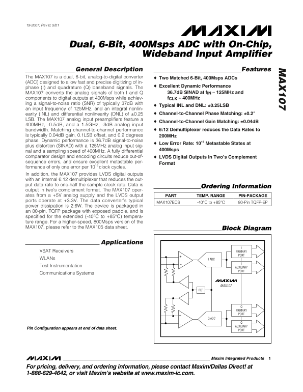
A high-performance dual 6-bit Analog-to-Digital Converter (ADC) designed for fast and accurate digitization of I/Q baseband signals up to 400Msps. Featuring an integrated wideband input amplifier, this component ensures excellent dynamic performance crucial for modern RF applications. The accompanying manual provides comprehensive technical specifications, pin diagrams, and detailed operating conditions required by engineers building sophisticated communication systems, including those used in WLANs, VSAT receivers, and test instrumentation.
Page 1 Text Content
19-2007; Rev 0; 5/01
Dual, 6-Bit, 400Msps ADC with On-Chip,
Wideband Input Amplifier
General Description Features
The MAX107 is a dual, 6-bit, analog-to-digital converter Two Matched 6-Bit, 400Msps ADCs (ADC) designed to allow fast and precise digitizing of in-
Excellent Dynamic Performance
phase (I) and quadrature (Q) baseband signals. The
MAX107 converts the analog signals of both I and Q 36.7d B SINAD at f IN ≈ 125MHz and
components to digital outputs at 400Msps while achiev- f CLK ≈ 400MHz
ing a signal-to-noise ratio (SNR) of typically 37d B with
Typical INL and DNL: ±0.25LSB
an input frequency of 125MHz, and an integral nonlin-
earity (INL) and differential nonlinearity (DNL) of ±0.25 Channel-to-Channel Phase Matching: ±0.2°
LSB. The MAX107 analog input preamplifiers feature a
Channel-to-Channel Gain Matching: ±0.04d B
400MHz, -0.5d B, and a 1.5GHz, -3d B analog input
bandwidth. Matching channel-to-channel performance 6:12 Demultiplexer reduces the Data Rates to
is typically 0.04d B gain, 0.1LSB offset, and 0.2 degrees 200MHz phase. Dynamic performance is 36.7d B signal-to-noise
Low Error Rate: 1016 Metastable States at
plus distortion (SINAD) with a 125MHz analog input sig-
400Msps
nal and a sampling speed of 400MHz. A fully differential comparator design and encoding circuits reduce out-of- LVDS Digital Outputs in Two’s Complement sequence errors, and ensure excellent metastable per-
Format
formance of only one error per 1016 clock cycles. In addition, the MAX107 provides LVDS digital outputs with an internal 6:12 demultiplexer that reduces the out- put data rate to one-half the sample clock rate. Data is
Ordering Information
output in two’s complement format. The MAX107 oper- ates from a +5V analog supply and the LVDS output PART TEMP. RANGE PIN-PACKAGE ports operate at +3.3V. The data converter’s typical
MAX107ECS -40°C to +85°C 80-Pin TQFP-EP
power dissipation is 2.6W. The device is packaged in an 80-pin, TQFP package with exposed paddle, and is specified for the extended (-40°C to +85°C) tempera- ture range. For a higher-speed, 800Msps version of the MAX107, please refer to the MAX105 data sheet.
Block Diagram
Applications
VSAT Receivers PRIMARY
WLANs I ADC Test Instrumentation
AUXILIARY PORT
Communications Systems
MAX107
PRIMARY PORT
Q ADC
AUXILIARY
Pin Configuration appears at end of data sheet.
Maxim Integrated Products
For pricing, delivery, and ordering information, please contact Maxim/Dallas Direct! at 1-888-629-4642, or visit Maxim’s website at www.maxim-ic.com.
Page Summary Contents For MAXIM MAX107 Dual, 6-Bit, 400Msps ADC with On-Chip, Wideband Input Amplifier Data Sheet
Manual Details
| Brand | Dual |
|---|---|
| Pages | 21 |
| File Size | 1.39 MB |
| Published | May 20, 2026 |
Enter the captcha to get the download link:
