# A B C D E F G H I J K L M N O P Q R S T U V W X Y Z

LINEAR TECHNOLOGY LTC6240 LTC6241 LTC6242 Data Sheet User Guide

Summary

These advanced Operational Amplifiers are a series of single, dual, or quad low-noise Op Amps designed for high-precision signal processing applications. Featuring ultra-low input bias current (1pA max), rail-to-rail outputs, and exceptionally low offset voltage, they maintain stable performance even in demanding environments. Ideal for sensitive front-end electronics, medical instrumentation, and photodiode amplifiers requiring both rapid speed (up to 18MHz) and minimal noise across wide temperature ranges.
📄 Preview PAGE OF 28

Page 1 Text Content

LTC6240/LTC6241/LTC6242 Single/Dual/Quad 18MHz, Low Noise, Rail-to-Rail Output,

CMOS Op Amps

FEATURES DESCRIPTIO

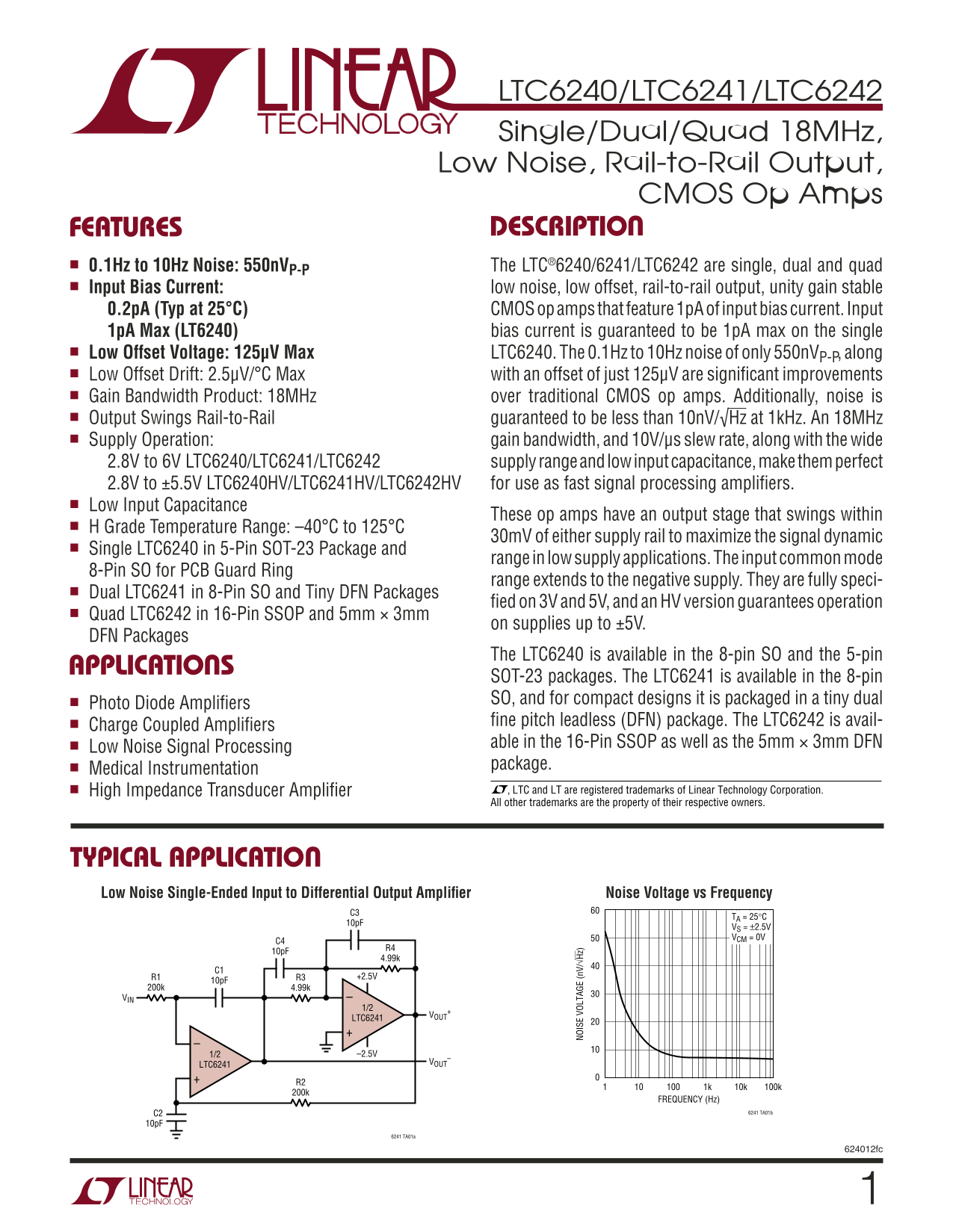
■ 0.1Hz to 10Hz Noise: 550n VP-P The LTC®6240/6241/LTC6242 are single, dual and quad ■ Input Bias Current: low noise, low offset, rail-to-rail output, unity gain stable 0.2p A (Typ at 25°C) CMOS op amps that feature 1p A of input bias current. Input 1p A Max (LT6240) bias current is guaranteed to be 1p A max on the single ■ Low Offset Voltage: 125µV Max LTC6240. The 0.1Hz to 10Hz noise of only 550n VP-P, along ■ Low Offset Drift: 2.5µV/°C Max with an offset of just 125µV are signifi cant improvements ■ Gain Bandwidth Product: 18MHz over traditional CMOS op amps. Additionally, noise is ■ Output Swings Rail-to-Rail guaranteed to be less than 10n V/√Hz at 1k Hz. An 18MHz ■ Supply Operation: gain bandwidth, and 10V/µs slew rate, along with the wide 2.8V to 6V LTC6240/LTC6241/LTC6242 supply range and low input capacitance, make them perfect 2.8V to ±5.5V LTC6240HV/LTC6241HV/LTC6242HV for use as fast signal processing amplifi ers. ■ Low Input Capacitance

These op amps have an output stage that swings within

■ H Grade Temperature Range: –40°C to 125°C

30m V of either supply rail to maximize the signal dynamic

■ Single LTC6240 in 5-Pin SOT-23 Package and

range in low supply applications. The input common mode

8-Pin SO for PCB Guard Ring

NO IS VO LT AG (n V/ √H z) range extends to the negative supply. They are fully speci-

■ Dual LTC6241 in 8-Pin SO and Tiny DFN Packages

fi ed on 3V and 5V, and an HV version guarantees operation

■ Quad LTC6242 in 16-Pin SSOP and 5mm × 3mm

on supplies up to ±5V.

DFN Packages

The LTC6240 is available in the 8-pin SO and the 5-pin

APPLICATIO

SOT-23 packages. The LTC6241 is available in the 8-pin ■ Photo Diode Amplifi ers SO, and for compact designs it is packaged in a tiny dual ■ Charge Coupled Amplifi ers fi ne pitch leadless (DFN) package. The LTC6242 is avail- ■ Low Noise Signal Processing able in the 16-Pin SSOP as well as the 5mm × 3mm DFN ■ Medical Instrumentation package.

■ High Impedance Transducer Amplifi er , LTC and LT are registered trademarks of Linear Technology Corporation.

All other trademarks are the property of their respective owners.

TYPICAL APPLICATIO Low Noise Single-Ended Input to Differential Output Amplifi er Noise Voltage vs Frequency

TA = 25°C

VS = ±2.5V VCM = 0V

200k 4.99k VIN

LTC6241

–1/2 LTC6241 VOUT

FREQUENCY (Hz)

C2 6241 TA01b

6241 TA01a

624012fc

Page Summary Contents For LINEAR TECHNOLOGY LTC6240 LTC6241 LTC6242 Data Sheet User Guide

Page 1 LTC6240/LTC6241/LTC6242 Single/Dual/Quad 18MHz, Low Noise, Rail-to-Rail Output, CMOS Op Amps FEATURES DESCRIPTIO ■ 0.1Hz to 10Hz Noise: 550n VP-P The LTC®6240/6241/LTC6242 are single, dual and quad ■ ...
Page 2 LTC6240/LTC6241/LTC6242 RATI GS (Note 1)ABSOLUTE AXI Total Supply Voltage (V+ to V–) Specifi ed Temperature Range (Note 3) LTC6240/LTC6241/LTC6242 ...................................7V LTC6240C/LTC624...
Page 3 LTC6240/LTC6241/LTC6242 UW PACKAGE/ORDER I FOR ATIO ORDER PART NUMBER DHC PART MARKING* TOP VIEW TOP VIEW LTC6242CDHC OUT A OUT D OUT A OUT D –IN A –IN D LTC6242HVCDHC 6242HV –IN A –IN D +IN A +IN D L...
Page 4 LTC6240/LTC6241/LTC6242 AVAILABLE OPTIO S PART NUMBER AMPS/PACKAGE SPECIFIED TEMP RANGE SPECIFIED SUPPLY VOLTAGE PACKAGE PART MARKING LTC6242CGN 0°C to 70°C 3V, 5V GN LTC6242CDHC 0°C to 70°C 3V, 5V DH...
Page 5 LTC6240/LTC6241/LTC6242 (LTC6240C/I, LTC6240HVC/I, LTC6241C/I, LTC6241HVC/I, LTC6242C/I, ELECTRICAL CHARACTERISTICS LTC6242HVC/I) The ● denotes the specifi cations which apply over the specifi ed temp...
Page 6 LTC6240/LTC6241/LTC6242 ELECTRICAL CHARACTERISTICS (LTC6240C/I, LTC6240HVC/I, LTC6241C/I, LTC6241HVC/I, LTC6242C/I, LTC6242HVC/I) The ● denotes the specifi cations which apply over the specifi ed temp...
Page 7 LTC6240/LTC6241/LTC6242 (LTC6240HVC/I, LTC6241HVC/I, LTC6242HVC/I) The ● denotes the ELECTRICAL CHARACTERISTICS specifi cations which apply over the specifi ed temperature range, otherwise specifi cat...
Page 8 LTC6240/LTC6241/LTC6242 (LTC6240HVC/I, LTC6241HVC/I, LTC6242HVC/I) The ● denotes the ELECTRICAL CHARACTERISTICS specifi cations which apply over the specifi ed temperature range, otherwise specifi cat...
Page 9 LTC6240/LTC6241/LTC6242 ELECTRICAL CHARACTERISTICS (LTC6240H/LTC6240HVH, LTC6241H/LTC6241HVH, LTC6242H/LTC6242HVH) The ● denotes the specifi cations which apply from –40°C to 125°C, otherwise specifi ...
Page 10 LTC6240/LTC6241/LTC6242 (LTC6240H/LTC6240HVH, LTC6241H/LTC6241HVH, LTC6242H/LTC6242HVH) ELECTRICAL CHARACTERISTICS The ● denotes the specifi cations which apply from –40°C to 125°C, otherwise specifi ...
Page 11 LTC6240/LTC6241/LTC6242 ELECTRICAL CHARACTERISTICS (LTC6240HVH/LTC6241HVH/LTC6242HVH) The ● denotes the specifi cations which apply from –40°C to 125°C, otherwise specifi cations are at TA = 25°C. VS ...
Page 12 OF FS ET OL TA GE (µ V) PE RC EN OF NI TS NU BE OF NI TS LTC6240/LTC6241/LTC6242 TYPICAL PERFOR A CE CHARACTERISTICS VOS Temperature Coeffi cient VOS Distribution LTC6241 VOS Distribution LTC6241 Dist...
Page 13 PHASE M ARGIN (DEG) GA IN AN DW ID TH (M Hz IN PU BI AS UR RE NT (p A) SL EW AT (V /µ s) LTC6240/LTC6241/LTC6242 TYPICAL PERFOR A CE CHARACTERISTICS Output Saturation Voltage vs Output Saturation Volt...
Page 14 IN PU VO LT AG (µ V) CH AN GE IN FF SE VO LT AG (µ V) VO LT AG GA IN (d B) LTC6240/LTC6241/LTC6242 TYPICAL PERFOR A CE CHARACTERISTICS Power Supply Rejection Ratio vs Channel Separation vs Frequency F...
Page 15 IS CU RR EN (f A /√ Hz CH AN GE IN FF SE VO LT AG (µ V) OV ER SH OO LTC6240/LTC6241/LTC6242 TYPICAL PERFOR A CE CHARACTERISTICS Warm-Up Drift vs Time Noise Voltage vs Frequency 0.1Hz to 10Hz Voltage N...
Page 16 DI ST OR TI ON (d Bc OU TP UT OL TA GE IN GI NG (V LTC6240/LTC6241/LTC6242 TYPICAL PERFOR A CE CHARACTERISTICS Maximum Undistorted Output Signal vs Frequency Distortion vs Frequency Distortion vs Freq...
Page 17 LTC6240/LTC6241/LTC6242 APPLICATIO S I FOR ATIO Amplifi er Characteristics The amplifi er input bias current is the leakage current of these ESD diodes. This leakage is a function of the tem- Figure 1...
Page 18 LTC6240/LTC6241/LTC6242 APPLICATIO S I FOR ATIO Proprietary design techniques are used to obtain simulta- Half the Noise neous low 1/f noise and low input capacitance. Low input The circuit shown in F...
Page 19 LTC6240/LTC6241/LTC6242 FF ER EN TI AL UT PU VO LT AG DE NS IT (n V/ √H z) APPLICATIO S I FOR ATIO phase lead to compensate the phase lag of the second source equal to the input voltage prevents such ...
Page 20 LTC6240/LTC6241/LTC6242 APPLICATIO S I FOR ATIO R3 V+ contribute any signifi cant error to the LT6650 reference 0.1µF voltage. The LT6650 VREF voltage has a maximum error V1 of ±2% with 1% resistors. ...
Page 21 LTC6240/LTC6241/LTC6242 APPLICATIO S I FOR ATIO to achieve an extraordinarily low noise and low DC drift. with the input chopper, proper amplitude and polarity The performance of this circuit is suite...
Page 22 LTC6240/LTC6241/LTC6242 APPLICATIO S I FOR ATIO The noise measured over a 50 second interval, in Figure 10, by the sensor is forced across the feedback capacitor is 40n V in a 0.1Hz to 10Hz bandwidth....
Page 23 LTC6240/LTC6241/LTC6242 APPLICATIO S I FOR ATIO 1M Transimpedance Amplifi er with 43n V/√Hz By achieving an output swing of 50V before attenuation, Output Noise the circuit provides an output swing to...
Page 24 LTC6240/LTC6241/LTC6242 PACKAGE DESCRIPTIO DHC Package 16-Lead Plastic DFN (5mm × 3mm) (Reference LTC DWG # 05-08-1706) 1.65 ±0.05 (2 SIDES)2.20 ±0.05 PACKAGE OUTLINE 0.25 ± 0.05 0.50 BSC 4.40 ±0.05 (...
Page 25 LTC6240/LTC6241/LTC6242 PACKAGE DESCRIPTIO DD Package 8-Lead Plastic DFN (3mm × 3mm) (Reference LTC DWG # 05-08-1698) (2 SIDES)2.15 ±0.05 (4 SIDES) (2 SIDES) PIN 1 TOP MARK PACKAGE (NOTE 6) OUTLINE (D...
Page 26 LTC6240/LTC6241/LTC6242 PACKAGE DESCRIPTIO S5 Package 5-Lead Plastic TSOT-23 (Reference LTC DWG # 05-08-1635) 2.90 BSC MAX REF (NOTE 4) 1.22 REF 3.85 MAX 1.4 MIN2.62 REF (NOTE 4)2.80 BSC PIN ONE RECOM...
Page 27 LTC6240/LTC6241/LTC6242 PACKAGE DESCRIPTIO S8 Package 8-Lead Plastic Small Outline (Narrow .150 Inch) (Reference LTC DWG # 05-08-1610) NOTE 3 .050 BSC MIN .150 – .157 NOTE 3 .030 ±.005 TYP RECOMMENDED...
Page 28 LTC6240/LTC6241/LTC6242 n V /√ Hz ER IV TYPICAL APPLICATIO 1MΩ TIA 150k Hz 3RD ORDER BUTTERWORTH FILTER 1/2 LTC6241 C1 C3 LTC6241 RF 1500p F 180p F 1M SFH213FA –1.5V OR EQUIVALENT 6241 TA02a Figure 15...

Manual Details

Brand Linear
Pages 28
File Size 529.32 KB
Published June 22, 2026
2 views

Enter the captcha to get the download link:

captcha

Frequently Asked Questions

What temperature range does the LTC6240HV/LTC6241HV/LTC6242HV series cover?

The 'H' grade versions are rated for operation in a wide temperature range of -40°C to 125°C.

What is the guaranteed input bias current for these op amps?

The low noise, low offset CMOS op amps guarantee an input bias current of 1pA max on the single LTC6240 model.

In what package options is the LTC6241 available?

The LTC6241 is available in an 8-pin SO, or in a tiny dual fine pitch leadless DFN package for compact designs.