# A B C D E F G H I J K L M N O P Q R S T U V W X Y Z

LINEAR TECHNOLOGY LTC1285 LTC1288 Data Sheet User Guide

Summary

Ideal for building low-power, battery-operated sensing equipment, these 12-bit micropower A/D converters provide high accuracy with ultra-low supply current consumption. Designed for remote data acquisition and systems requiring single-supply operation (3V–6V), they feature advanced capabilities like auto-shutdown to conserve power for demanding applications such as temperature monitoring. This guide covers technical specifications, integration details for both single differential inputs and dual multiplexing, and guidelines for system designers implementing reliable, high-precision signal capture.
📄 Preview PAGE OF 24

Page 1 Text Content

LTC1285/LTC1288 3V Micropower Sampling 12-Bit A/D Converters in SO-8 Packages

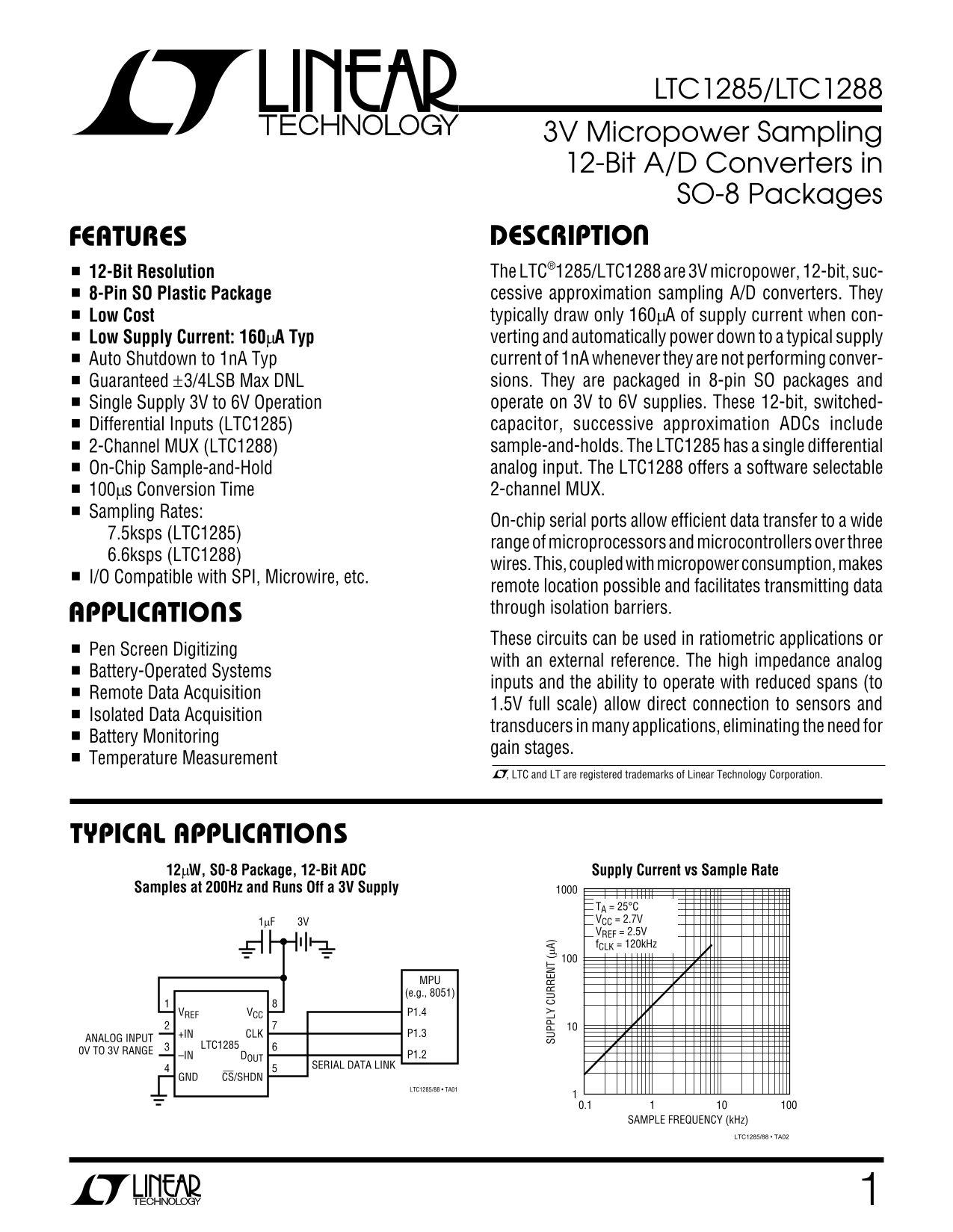
FEATURES DESCRIPTION 12-Bit Resolution The LTC®1285/LTC1288 are 3V micropower, 12-bit, suc- 8-Pin SO Plastic Package cessive approximation sampling A/D converters. They Low Cost typically draw only 160µA of supply current when con- Low Supply Current: 160µA Typ verting and automatically power down to a typical supply Auto Shutdown to 1n A Typ current of 1n A whenever they are not performing conver- Guaranteed ±3/4LSB Max DNL sions. They are packaged in 8-pin SO packages and Single Supply 3V to 6V Operation operate on 3V to 6V supplies. These 12-bit, switched- Differential Inputs (LTC1285) capacitor, successive approximation ADCs include 2-Channel MUX (LTC1288) sample-and-holds. The LTC1285 has a single differential On-Chip Sample-and-Hold analog input. The LTC1288 offers a software selectable 100µs Conversion Time 2-channel MUX.

Sampling Rates:

On-chip serial ports allow efficient data transfer to a wide

7.5ksps (LTC1285)

range of microprocessors and microcontrollers over three

SU PP LY UR RE NT (µ A)

6.6ksps (LTC1288)

wires. This, coupled with micropower consumption, makes

I/O Compatible with SPI, Microwire, etc.

remote location possible and facilitates transmitting data through isolation barriers.

APPLICATIONS

These circuits can be used in ratiometric applications or

Pen Screen Digitizing

with an external reference. The high impedance analog

Battery-Operated Systems

inputs and the ability to operate with reduced spans (to

Remote Data Acquisition

1.5V full scale) allow direct connection to sensors and

Isolated Data Acquisition

transducers in many applications, eliminating the need for

Battery Monitoring

gain stages.

Temperature Measurement

, LTC and LT are registered trademarks of Linear Technology Corporation.

TYPICAL APPLICATIONS N 12µW, S0-8 Package, 12-Bit ADC Supply Current vs Sample Rate Samples at 200Hz and Runs Off a 3V Supply

TA = 25°C 3V1µF VCC = 2.7V VREF = 2.5V f CLK = 120k Hz

MPU (e.g., 8051)

VREF VCC P1.4

+IN CLK P1.3

ANALOG INPUT

LTC1285

0V TO 3V RANGE

–IN DOUT P1.2

SERIAL DATA LINK

GND CS/SHDN

LTC1285/88 • TA01

SAMPLE FREQUENCY (k Hz)

LTC1285/88 • TA02

Page Summary Contents For LINEAR TECHNOLOGY LTC1285 LTC1288 Data Sheet User Guide

Page 1 LTC1285/LTC1288 3V Micropower Sampling 12-Bit A/D Converters in SO-8 Packages FEATURES DESCRIPTION 12-Bit Resolution The LTC®1285/LTC1288 are 3V micropower, 12-bit, suc- 8-Pin SO Plastic Package cessi...
Page 2 LTC1285/LTC1288 ABSOLUTE MAXIMUM RATINGS (Notes 1 and 2) Supply Voltage (VCC) to GND................................... 12V Power Dissipation 500m W Voltage Operating Temperature Range 0°C to 70°C Ana...
Page 3 LTC1285/LTC1288 CONVERTER AND MULTIPLEXER CHARACTERISTICS (Note 5) LTC1285 LTC1288 PARAMETER CONDITIONS MIN TYP MAX MIN TYP MAX UNITS Resolution (No Missing Codes) Bits Integral Linearity Error (Note ...
Page 4 SU PP LY UR RE NT (µ A) LTC1285/LTC1288 (Note 5)AC CHARACTERISTICS SYMBOL PARAMETER CONDITIONS MIN TYP MAX UNITS t SMPL Analog Input Sample Time See Operating Sequence 1.5 CLK Cycles f SMPL (MAX) Maxi...
Page 5 CH AN GE IN FF SE (L SB RE FE RE NC CU RR EN (µ A) LTC1285/LTC1288 TYPICAL PERFORMANCE CHARACTERISTICS DI FF ER EN TI AL ON LI NE AR IT ER RO (L SB S/(N + D) (d B) Reference Current vs Change in Offse...
Page 6 AG NI TU DE (d B) CL OC FR EQ UE NC (k Hz SP UR IO US -F RE DY NA IC AN GE (d B) LTC1285/LTC1288 TYPICAL PERFORMANCE CHARACTERISTICS Spurious-Free Dynamic Range vs Input Frequency S/(N + D) vs Input L...
Page 7 CL OC FR EQ UE NC (k Hz LTC1285/LTC1288 TYPICAL PERFORMANCE CHARACTERISTICS Minimum Clock Frequency Digital Input Logic Threshold Input Channel Leakage Current for 0.1 LSB Error vs Temperature vs Supp...
Page 8 LTC1285/LTC1288 BLOCK DIAGRAM CS/SHDN (DIN) CLK VCC (VCC/VREF) BIAS AND SERIAL PORT DOUT SHUTDOWN CIRCUIT IN+ (CH0) CSAMPLE IN– (CH1) MICROPOWER COMPARATOR CAPACITIVE DAC LTC1285/88 • BD GND VREF PIN ...
Page 9 LTC1285/LTC1288 TEST CIRCUITS Voltage Waveforms for tdis Voltage Waveforms for ten LTC1285 CS VIH CS WAVEFORM 1 (SEE NOTE 1) DOUT WAVEFORM 2 (SEE NOTE 2) NOTE 1: WAVEFORM 1 IS FOR AN OUTPUT WITH INTER...
Page 10 LTC1285/LTC1288 APPLICATION INFORMATION OVERVIEW basic design, the LTC1285 and LTC1288 differ in some respects. The LTC1285 has a differential input and has an The LTC1285 and LTC1288 are 3V micropowe...
Page 11 LTC1285/LTC1288 APPLICATION INFORMATION MSB-First Data (MSBF = 0) t CYC tsu CS POWER DOWN START SIGN DIN DON’T CARE SGL/ MSBF DIFF NULL HI-Z BIT HI-ZDOUT t SMPL (MSB) t CONV t DATA MSB-First Data (MSB...
Page 12 LTC1285/LTC1288 APPLICATION INFORMATION Data Transfer the rising edge of the clock. The input data words are defined as follows: The CLK synchronizes the data transfer with each bit being transmitted ...
Page 13 LTC1285/LTC1288 APPLICATION INFORMATION Transfer Curve either an input or an output. The LTC1288 will take control of the data line and drive it low on the 4th falling CLK edge The LTC1285/LTC1288 are...
Page 14 LTC1285/LTC1288 SU PP LY UR RE NT (µ A) APPLICATION INFORMATION Several things must be taken into account to achieve such lowest current drain. This minimizes the amount of time a low power consumptio...
Page 15 LTC1285/LTC1288 APPLICATION INFORMATION of Maximum Clock Rate vs Supply Voltage). If the maxi- BOARD LAYOUT CONSIDERATIONS mum clock frequency is used, care must be taken to ensure that the device con...
Page 16 LTC1285/LTC1288 APPLICATION INFORMATION Single-Ended Inputs “+” Input Settling The sample-and-hold of the LTC1288 allows conversion The input capacitor of the LTC1285 is switched onto “+” of rapidly v...
Page 17 LTC1285/LTC1288 APPLICATION INFORMATION selected “+” and “–” inputs once during each conversion Input Leakage Current cycle. Large external source resistors and capacitances Input leakage currents can...
Page 18 LTC1285/LTC1288 APPLICATION INFORMATION Voltage). However, care must be taken when operating at noise becomes equal to 3.3LSBs and a stable code may low values of VREF because of the reduced LSB step ...
Page 19 LTC1285/LTC1288 EF FE CT IV BE BI TS EN Bs APPLICATION INFORMATION Signal-to-Noise Ratio The Signal-to-Noise plus Distortion Ratio (S/N + D) is the THD 20log ratio between the RMS amplitude of the fun...
Page 20 LTC1285/LTC1288 TYPICAL APPLICATIONS N MICROPROCESSOR INTERFACES Table 1. Microprocessor with Hardware Serial Interfaces Compatible with the LTC1286/LTC1298 The LTC1285/LTC1288 can interface directly ...
Page 21 LTC1285/LTC1288 TYPICAL APPLICATIONS N Timing Diagram for Interface to the MC68HC11 DIN MSBF DON'T CAREODD/ DIFFSTART SIGN TRANSMIT MSBF XODD/ XX0 XX XX DIFF SIGN BYTE 1 BYTE 3 (DUMMY)BYTE 2 RECEIVED ...
Page 22 LTC1285/LTC1288 TYPICAL APPLICATIONS N Interfacing to the Parallel Port of the INTEL 8051 LABEL MNEMONIC OPERAND COMMENTS Family MOV A, #FFH DIN word for LTC1288 SETB P1.4 Make sure CS is high The Int...
Page 23 LTC1285/LTC1288 TYPICAL APPLICATIONS N A “Quick Look” Circuit for the LTC1285 Micropower Battery Voltage Monitor Users can get a quick look at the function and timing of the A common problem in batter...
Page 24 LTC1285/LTC1288 Dimensions in inches (millimeters) unless otherwise noted.PACKAGE DESCRIPTION N8 Package 8-Lead Plastic DIP 0.400* (10.160) 0.300 – 0.325 0.045 – 0.065 0.130 ± 0.005 MAX 0.009 – 0.015 ...

Manual Details

Brand Linear
Pages 24
File Size 342.49 KB
Published July 16, 2026
0 views

Enter the captcha to get the download link:

captcha

Frequently Asked Questions

What is the maximum supply current?

The device typically draws only 160μA of supply current and can auto-shutdown to a typical current of 1nA.

Which model has a built-in multiplier (MUX)?

The LTC1288 offers a software selectable 2-channel MUX, while the LTC1285 has a single differential analog input.

What are these chips compatible with in data transmission?

They are compatible with SPI, Microwire, etc., allowing for efficient data transfer to microprocessors and microcontrollers.

What voltage range can the device operate on?

The devices operate on a single supply voltage ranging from 3V to 6V.