# A B C D E F G H I J K L M N O P Q R S T U V W X Y Z

LINEAR TECHNOLOGY LTC3738 Owner's Manual User Guide

Summary

This advanced 3-phase synchronous step-down regulator controller features programmable Active Voltage Positioning (AVP) to optimize power delivery efficiency for demanding computing systems like servers, workstations, and high-performance laptops. The LTC3738 provides precise output current matching with built-in protections, including adjustable thermal detection and short-circuit shutdown. It is designed for engineers who require a highly reliable, expandable solution capable of meeting the stringent power requirements of modern multi-CPU and fast-transient load environments.
📄 Preview PAGE OF 32

Page 1 Text Content

LTC3738

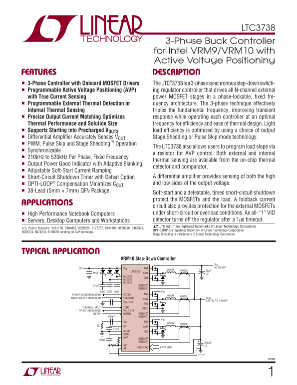
3-Phase Buck Controller for Intel VRM9/VRM10 with Active Voltage Positioning

FEATURES DESCRIPTIO 3-Phase Controller with Onboard MOSFET Drivers The LTC®3738 is a 3-phase synchronous step-down switch- Programmable Active Voltage Positioning (AVP) ing regulator controller that drives all N-channel external with True Current Sensing power MOSFET stages in a phase-lockable, fixed fre- Programmable External Thermal Detection or quency architecture. The 3-phase technique effectively Internal Thermal Sensing triples the fundamental frequency, improving transient Precise Output Current Matching Optimizes response while operating each controller at an optimal Thermal Performance and Solution Size frequency for efficiency and ease of thermal design. Light

Supports Starting into Precharged VOUTS load efficiency is optimized by using a choice of output Differential Amplifier Accurately Senses VOUT Stage Shedding or Pulse Skip mode technology.

PWM, Pulse Skip and Stage Shedding TM Operation

The LTC3738 also allows users to program load slope via

Synchronizable

a resistor for AVP control. Both external and internal

210k Hz to 530k Hz Per Phase, Fixed Frequency

thermal sensing are available from the on-chip thermal

Output Power Good Indicator with Adaptive Blanking

detector and comparator.

Adjustable Soft-Start Current Ramping

Short-Circuit Shutdown Timer with Defeat Option A differential amplifier provides sensing of both the high OPTI-LOOP® Compensation Minimizes COUT and low sides of the output voltage.

38-Lead (5mm × 7mm) QFN Package

Soft-start and a defeatable, timed short-circuit shutdown protect the MOSFETs and the load. A foldback current

APPLICATIO

circuit also provides protection for the external MOSFETs High Performance Notebook Computers under short-circuit or overload conditions. An all- “1” VID Servers, Desktop Computers and Workstations detector turns off the regulator after a 1µs timeout. , LTC and LT are registered trademarks of Linear Technology Corporation.

U.S. Patent Numbers: 5481178, 5994885, 5929620, 6177787, 6144194, 6580258, 6462525,

OPTI-LOOP is a registered trademark of Linear Technology Corporation.

6593724, 6674274, 6100678 pending on AVP technique.

Stage Shedding is a trademark of Linear Technology Corporation.

TYPICAL APPLICATIO

VRM10 Step-Down Controller

VIN 5V TG1VCC 5V TO 28V

LTC3738 0.002Ω0.8µH 22µF

10µF SW1 ×2

BOOST1

BOOST2 BOOST3

0.1µF SENSE1+ SENSE1–

SW3 SW2 SW1 VIN

POWER GOOD INDICATOR PGOOD TG2

FCB/SYNCMODE SELECTION/SYNC IN VOUT

0.8375V TO 1.6000V

PLLFLTR

TSNSTHERMAL INPUT

VR_HOTBVR HOT INDICATOR

ON/OFF OUTEN SENSE2+

680p F SENSE2–

ITH TG3

5k SS

SGND BG3 EAIN AVP

SENSE3+

SENSE3–

IN+ ×4

VID0-VID5 6 VID BITS

3738 TA01

Page Summary Contents For LINEAR TECHNOLOGY LTC3738 Owner's Manual User Guide

Page 1 LTC3738 3-Phase Buck Controller for Intel VRM9/VRM10 with Active Voltage Positioning FEATURES DESCRIPTIO 3-Phase Controller with Onboard MOSFET Drivers The LTC®3738 is a 3-phase synchronous step-down ...
Page 2 LTC3738 ABSOLUTE AXI U RATI GS PACKAGE/ORDER I FOR ATIO (Note 1) Topside Driver Voltages (BOOSTN) 38V to –0.3V TOP VIEW Switch Voltage (SWN)................................... 32V to –5V Boosted Drive...
Page 3 LTC3738 ELECTRICAL CHARACTERISTICS The ● denotes the specifications which apply over the full operating temperature range, otherwise specifications are at TA = 25°C. VCC = VOUTEN = VSS = 5V unless oth...
Page 4 LTC3738 ELECTRICAL CHARACTERISTICS The ● denotes the specifications which apply over the full operating temperature range, otherwise specifications are at TA = 25°C. VCC = VOUTEN = VSS = 5V unless oth...
Page 5 FR EQ UE NC (k Hz RE FE RE NC VO LT AG (m V) EF FI CI EN CY LTC3738 TYPICAL PERFOR A CE CHARACTERISTICS TA = 25°C unless otherwise noted. Efficiency vs IOUT Efficiency vs VIN Efficiency vs Frequency V...
Page 6 PE AK EN SE OL TA GE (m V) SS UL L- UP UR RE NT (µ A) SS IN OL TA GE (V LTC3738 TYPICAL PERFOR A CE CHARACTERISTICS TA = 25°C unless otherwise noted. Short-Circuit Arming and Latchoff Shutdown Current...
Page 7 LTC3738 TYPICAL PERFOR A CE CHARACTERISTICS TA = 25°C unless otherwise noted. AX IM UM UR RE NT HR ES HO LD IS AT CH (m V) +) vs Maximum Current Threshold (VAVP – VIN + – VSENSE –) Mismatch vs Tempera...
Page 8 LTC3738 PI FU CTIO S FCB/SYNC (Pin 1): Forced Continuous Control Input. The SS (Pin 13): Combination of Soft-Start and Short-Circuit voltage applied to this pin sets the operating mode of the Detectio...
Page 9 LTC3738 PI FU CTIO S SW1, SW2, SW3 (Pins 30, 27, 21): Switch Node Connec- PGOOD (Pin 33): This open-drain output is pulled low tions to Inductors. Voltage swing at these pins is from a when the output...
Page 10 LTC3738 FU CTIO AL DIAGRA PGOOD 0.66V VR_HOTB 100µs TCMP BLANKING FCB/SYNC +VCC/3 VID TRANSITIONS 0.54V MUX FCB INTERNAL 0.6V THERMAL DETECTION PHASE DET RLP PLLFLTR VCC VIN DUPLICATE FOR SECOND AND T...
Page 11 LTC3738 OPERATIO (Refer to Functional Diagram) Main Control Loop Low Current Operation The IC uses a constant frequency, current mode step- The FCB/SYNC pin is a multifunction pin: 1) a logic input do...
Page 12 LTC3738 OPERATIO (Refer to Functional Diagram) Tying the FCB/SYNC pin to ground will force continuous Power Good current operation. This is the least efficient operating The PGOOD pin is connected to ...
Page 13 LTC3738 OPERATIO (Refer to Functional Diagram) Start-Up Thermal Detection The start-up of the LTC3738 is controlled by the voltage An accurate comparator and a thermal detector are inte- ramp on the S...
Page 14 LTC3738 OP ER AT IN FR EQ UE NC (k Hz APPLICATIO S I FOR ATIO The basic application circuit is shown on the first page of Inductor Value Calculation and Output Ripple Current this data sheet. External...
Page 15 LTC3738 APPLICATIO S I FOR ATIO 1.0 1-PHASE Ferrite designs have very low core loss and are preferred 0.9 2-PHASE 3-PHASE at high switching frequencies, so design goals can 4-PHASE concentrate on copp...
Page 16 LTC3738 APPLICATIO S I FOR ATIO The power dissipation for the main and synchronous MILLER EFFECT MOSFETs at maximum output current are given by: OUT MAX MAIN DS ON CMILLER = (QB – QA)/VDS 3738 F04 IN ...
Page 17 LTC3738 APPLICATIO S I FOR ATIO The Schottky diodes shown in the Typical Application on These worst-case conditions are commonly used for de- the first page of this data sheet conduct during the dead ...
Page 18 LTC3738 APPLICATIO S I FOR ATIO applied. Physically, if the capacitance value changes due hole capacitors. The OS-CON semiconductor dielectric to applied voltage change, there is a concommitant piezo ...
Page 19 LTC3738 APPLICATIO S I FOR ATIO VCC Decoupling common, tightly coupled pair of PC traces. The differen- tial amplifier rejects common mode signals capacitively The VCC pin supplies power not only to t...
Page 20 LTC3738 APPLICATIO S I FOR ATIO Table 1. VRM9 VID Table Thermal Control PROCESSOR PINS (0 = L0W, 1 = HIGH) VCC(CORE) When external thermal detection is enabled, the TSNS pin VID4 VID3 VID2 VID1 VID0 (...
Page 21 LTC3738 Table 2. VRM10 VID Table PROCESSOR PINS (0 = LOW, 1 = HIGH) VOUT PROCESSOR PINS (0 = LOW, 1 = HIGH) VOUT VID4 VID3 VID2 VID1 VID0 VID5 VID4 VID3 VID2 VID1 VID0 VID5 0.8375 1.2125 0.8500 1.2250...
Page 22 LTC3738 APPLICATIO S I FOR ATIO given adequate time to charge up the output capacitor and The value of the soft-start capacitor CSS may need to be provide full load current, the SS capacitor is used f...
Page 23 LTC3738 APPLICATIO S I FOR ATIO Undervoltage Reset PHASE 2.4V DETECTOR/ In the event that the input power source to the IC (VCC) CLP OSCILLATOR EXTERNAL drops below 4V, the SS capacitor will be discha...
Page 24 LTC3738 APPLICATIO S I FOR ATIO If the duty cycle falls below what can be accommodated by time, VOUT can be monitored for excessive overshoot or the minimum on-time, the IC will begin to skip every ot...
Page 25 LTC3738 APPLICATIO S I FOR ATIO alter its delivery of current quickly enough to prevent this Next verify the minimum on-time is not violated. The sudden step change in output voltage if the load switc...
Page 26 LTC3738 APPLICATIO S I FOR ATIO PC Board Layout Checklist 6) The filter capacitors between the ITH and SGND pins should be as close as possible to the pins of the IC. When laying out the printed circu...
Page 27 LTC3738 APPLICATIO S I FOR ATIO SW1 RSENSE1 L2 VOUT SW2 RSENSE2 CIN D2 COUT BOLD LINES INDICATE HIGH, SWITCHING CURRENT LINES. L3 KEEP LINES TO A MININMUM LENGTH SW3 RSENSE3 Figure 9. Branch Current W...
Page 28 LTC3738 APPLICATIO S I FOR ATIO SINGLE PHASE subtract current from the (VCC – VOUT)/L charging current SW V resulting from the stage which has its top MOSFET on. The output ripple current for a 3-phas...
Page 29 LTC3738 APPLICATIO S I FOR ATIO result that is within 10% to 20% of the final application. This totals 0.14W at VIN = 8V, 0.315W at VIN = 12V and The temperature of the MOSFET’s die temperature may 0....
Page 30 LTC3738 TYPICAL APPLICATIO 65A Power Supply for VRM10 VCC 5V PGOOD 1Ω VID2 IN VID0 IN VCC VID5 INVID1 INON/0FF 51k100p F 0.1µF VIN OUTEN VID2 VID1 VID0 PGOODVID5 BOOST1 VOUT FCB/SYNC TG1 M1 L1 PLLFLTR...
Page 31 LTC3738 PACKAGE DESCRIPTIO UHF Package 38-Lead Plastic QFN (7mm × 5mm) (Reference LTC DWG # 05-08-1701) 5.50 ± 0.05 (2 SIDES) 4.10 ± 0.05 (2 SIDES) 3.20 ± 0.05 (2 SIDES) PACKAGE OUTLINE 0.25 ± 0.05 0....
Page 32 LTC3738 RELATED PARTS PART NUMBER DESCRIPTION COMMENTS LTC1628/LTC1628-PG/ 2-Phase, Dual Output Synchronous Step-Down Reduces CIN and COUT, Power Good Output Signal, Synchronizable, LTC1628-SYNC DC/DC...