# A B C D E F G H I J K L M N O P Q R S T U V W X Y Z

LINEAR TECHNOLOGY LT1398 LT1399 LT1399HV Owner's Manual

Summary

The LT1398/LT1399/LT1399HV provides low-cost, high-performance current feedback amplifiers with 300MHz bandwidth and independent channel control. Ideal for engineers developing portable equipment, video multiplexers, or broadcast systems, these chips offer fast switching, robust shutdown features, and operate across wide supply ranges (-2V to 15V). This manual provides comprehensive technical data sheets, electrical specifications, and example circuits necessary for integrating high-speed signal conditioning into demanding professional applications.
📄 Preview PAGE OF 16

Page 1 Text Content

LT1398/LT1399/LT1399HV Low Cost Dual and Triple 300MHz Current Feedback Amplifiers with Shutdown

FEATURES DESCRIPTIO 300MHz Bandwidth on ±5V (AV = 1, 2 and –1)

The LT®1399 and LT1399HV contain three independent

0.1d B Gain Flatness: 150MHz (AV = 1, 2 and –1)

300MHz current feedback amplifiers, each with a shut-

Completely Off in Shutdown, 0µA Supply Current

down pin. The LT1399HV is a higher voltage version of the

High Slew Rate: 800V/µs

LT1399. The LT1398 is a two amplifier version of the

Wide Supply Range:

LT1399.

±2V(4V) to ±6V(12V) (LT1398/LT1399)

The LT1398/LT1399 operate on all supplies from a single

±2V (4V) to ±7.5V (15V) (LT1399HV)

4V to ±6V. The LT1399HV operates on all supplies from 4V

80m A Output Current

to ±7.5V.

Low Supply Current: 4.6m A/Amplifier Fast Turn-On Time: 30ns Each amplifier draws 4.6m A when active. When disabled Fast Turn-Off Time: 40ns each amplifier draws zero supply current and its output be- 16-Pin Narrow SO/Narrow SSOP Packages comes high impedance. The amplifiers turn on in only 30ns

and turn off in 40ns, making them ideal in spread spectrum

APPLICATIO S

and portable equipment applications.

RGB Cable Drivers The LT1398/LT1399/LT1399HV are manufactured on Lin- LCD Drivers ear Technology’s proprietary complementary bipolar pro- Spread Spectrum Amplifiers cess. The LT1399/LT1399HV are pin-for-pin upgrades to MUX Amplifiers the LT1260 optimized for use on ±5V/±7.5V supplies.

Composite Video Cable Drivers , LTC and LT are registered trademarks of Linear Technology Corporation.

Portable Equipment

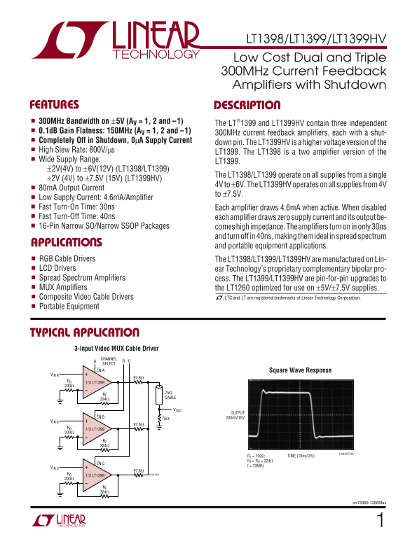
TYPICAL APPLICATIO 3-Input Video MUX Cable Driver

CCHANNEL

SELECT EN A Square Wave Response

VIN A

1/3 LT1399RG

CABLE

OUTPUT

EN B 75Ω 200m V/DIV

VIN B

1/3 LT1399RG

RF 324Ω

1398/99 TA02RL = 100Ω

TIME (10ns/DIV)

RF = RG = 324Ω

f = 10MHz

VIN C

97.6Ω 1399 TA01

1/3 LT1399RG

RF 324Ω

sn13989 13989fas

Page Summary Contents For LINEAR TECHNOLOGY LT1398 LT1399 LT1399HV Owner's Manual

Page 1 LT1398/LT1399/LT1399HV Low Cost Dual and Triple 300MHz Current Feedback Amplifiers with Shutdown FEATURES DESCRIPTIO 300MHz Bandwidth on ±5V (AV = 1, 2 and –1) The LT®1399 and LT1399HV contain three i...
Page 2 LT1398/LT1399/LT1399HV XI ARBSOLUTE TI (Note 1) + to V –) Total Supply Voltage (V Output Short-Circuit Duration (Note 3) Continuous LT1398/LT1399 12.6V Operating Temperature Range (Note 9) –40°C to 85...
Page 3 LT1398/LT1399/LT1399HV ELECTRICAL CHARA TERISTICS (LT1398/LT1399) The ● denotes specifications which apply over the specified operating temperature range, otherwise specifications are at TA = 25°C. Fo...
Page 4 LT1398/LT1399/LT1399HV ELECTRICAL CHARA TERISTICS (LT1399HV) The ● denotes specifications which apply over the specified operating temperature range, otherwise specifications are at TA = 25°C. For eac...
Page 5 LT1398/LT1399/LT1399HV ELECTRICAL CHARA TERISTICS (LT1399HV) The ● denotes specifications which apply over the specified operating temperature range, otherwise specifications are at TA = 25°C. For eac...
Page 6 DI ST OR TI ON (d B) GA IN (d B) OU TP UT (1 V/ DI V) LT1398/LT1399/LT1399HV PERFOR ATYPICAL CE CHARA TERISTICS Closed-Loop Gain vs Frequency Closed-Loop Gain vs Frequency Closed-Loop Gain vs Frequenc...
Page 7 OU TP UT OL TA GE IN (V CA PA CI TI VE OA (p F) IN PU NO IS (n V/ √H OR A/ √H z) LT1398/LT1399/LT1399HV PERFOR ATYPICAL CE CHARA TERISTICS Input Voltage Noise and Current Output Impedance (Disabled) N...
Page 8 LT1398/LT1399/LT1399HV PERFOR ATYPICAL CE CHARA TERISTICS AL HO ST IL CR OS ST AL (d B) IN PU OF FS ET OL TA GE (m V) Input Offset Voltage Input Bias Currents vs Temperature vs Temperature 3.0 VS = ±5...
Page 9 LT1398/LT1399/LT1399HV PIN FUNCTIONS LT1398 LT1399, LT1399HV –IN A (Pin 1): Inverting Input of A Channel Amplifier. –IN R (Pin 1): Inverting Input of R Channel Amplifier. IN A (Pin 2): Noninverting In...
Page 10 LT1398/LT1399/LT1399HV PPLICATI SA FOR ATIO Power Supplies will remain enabled at all times, then the EN pin should be – supply. The enable pin current is approxi- tied to the V The LT1398/LT1399 will...
Page 11 LT1398/LT1399/LT1399HV PPLICATI SA FOR ATIO The enable/disable times are very fast when driven from standard 5V CMOS logic. Each amplifier enables in about 30ns (50% point to 50% point) while operatin...
Page 12 LT1398/LT1399/LT1399HV PPLICATI SA FOR ATIO resistor R11, which yields a 75Ω input impedance at the R input when considered in parallel with R8. R8 connects to the inverting input of a second LT1398 a...
Page 13 LT1398/LT1399/LT1399HV PPLICATI SA FOR ATIO The G input also arrives via 75Ω coax and adds its R10, giving an amplification of – 0.37. This results in a contribution to the Y signal via a 549Ω resisto...
Page 14 LT1398/LT1399/LT1399HV SI PLIFIED SCHE ATIC , each amplifier +IN –IN OUT 1398/99 SS sn13989 13989fas
Page 15 LT1398/LT1399/LT1399HV Dimensions in inches (millimeters) unless otherwise noted.PACKAGE DESCRIPTIO GN Package 16-Lead Plastic SSOP (Narrow 0.150) (LTC DWG # 05-08-1641) 0.009 (0.229) REF 0° – 8° TYP0...
Page 16 LT1398/LT1399/LT1399HV PPLICATITYPICAL Single Supply RGB Video Amplifier input. Assuming a 75Ω source impedance for the signal driving VIN, the Thevenin equivalent signal arriving at The LT1399 can be...

Manual Details

Brand Linear
Pages 16
File Size 423.46 KB
Published June 21, 2026
8 views

Enter the captcha to get the download link:

captcha

Frequently Asked Questions

What are the operating temperature ranges for these amplifiers?

The specified operating temperature range is –40°C to 85°C, and the junction temperature maximum (JMAX JA T) is 150°C.

How do I ensure good channel isolation?

For best channel isolation, ground pins should be connected to ground.

What are the current consumption details?

Each amplifier draws 4.6mA when active and zero supply current when disabled (Shutdown Mode).

Are there differences between LT1398/LT1399 and the LT1399HV?

The LT1399HV is a higher voltage version, offering a wider operating supply range up to 15V.