# A B C D E F G H I J K L M N O P Q R S T U V W X Y Z

LINEAR TECHNOLOGY LTC2601 Data Sheet User Guide LTC2611 LTC2621

Summary

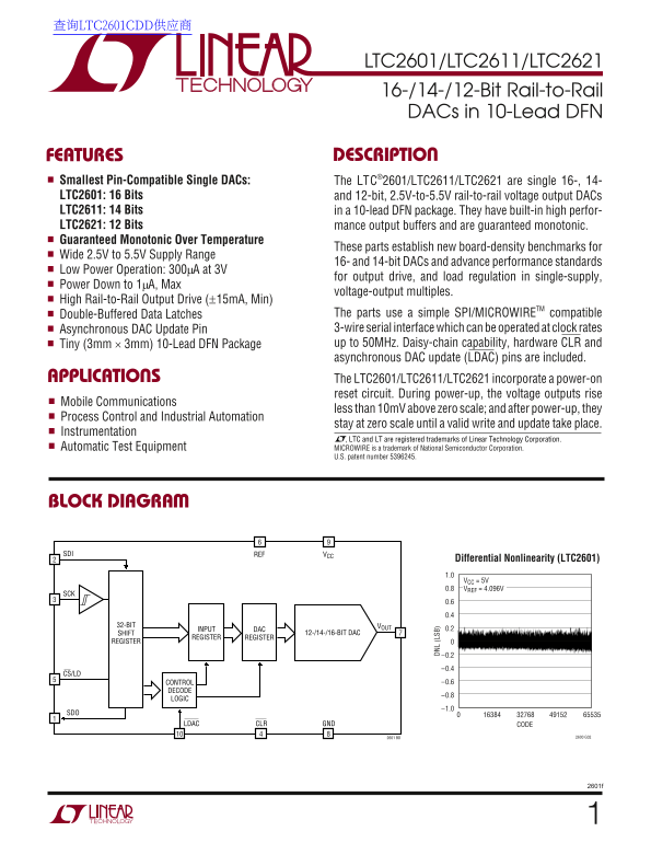
These compact, high-performance single DACs are ideal for advanced electronics in industrial automation, process control, and mobile communications. The LTC2601/LTC2611/LTC2621 series offers 16-, 14-, or 12-bit precision with rail-to-rail outputs and guaranteed monotonic performance across wide supply ranges (2.5V to 5.5V). This manual provides detailed electrical specifications, features low power consumption, and outlines simple SPI/MICROWIRE interfacing for system integration by professional design engineers.
📄 Preview PAGE OF 16

Page 1 Text Content

查询LTC2601CDD供应商

LTC2601/LTC2611/LTC2621 16-/14-/12-Bit Rail-to-Rail DACs in 10-Lead DFN

FEATURES DESCRIPTIO

Smallest Pin-Compatible Single DACs: The LTC®2601/LTC2611/LTC2621 are single 16-, 14- LTC2601: 16 Bits and 12-bit, 2.5V-to-5.5V rail-to-rail voltage output DACs LTC2611: 14 Bits in a 10-lead DFN package. They have built-in high perfor- LTC2621: 12 Bits mance output buffers and are guaranteed monotonic. Guaranteed Monotonic Over Temperature

These parts establish new board-density benchmarks for

Wide 2.5V to 5.5V Supply Range

16- and 14-bit DACs and advance performance standards

Low Power Operation: 300µA at 3V

for output drive, and load regulation in single-supply,

Power Down to 1µA, Max

voltage-output multiples.

High Rail-to-Rail Output Drive (±15m A, Min)

Double-Buffered Data Latches The parts use a simple SPI/MICROWIRETM compatible Asynchronous DAC Update Pin 3-wire serial interface which can be operated at clock rates Tiny (3mm × 3mm) 10-Lead DFN Package up to 50MHz. Daisy-chain capability, hardware CLR and asynchronous DAC update (LDAC) pins are included.

APPLICATIO The LTC2601/LTC2611/LTC2621 incorporate a power-on

reset circuit. During power-up, the voltage outputs rise

Mobile Communications

less than 10m V above zero scale; and after power-up, they

Process Control and Industrial Automation

stay at zero scale until a valid write and update take place.

Instrumentation

DN (L SB , LTC and LT are registered trademarks of Linear Technology Corporation.

Automatic Test Equipment MICROWIRE is a trademark of National Semiconductor Corporation.

U.S. patent number 5396245.

BLOCK DIAGRA

SDI REF VCC

Differential Nonlinearity (LTC2601) 1.0 VCC = 5V 0.8 VREF = 4.096V

32-BIT VOUT

INPUT DAC 0.2

SHIFT 12-/14-/16-BIT DAC

REGISTER REGISTER

REGISTER

CS/LD

CONTROL –0.6

DECODE

LOGIC

LDAC CLR GND CODE

2601 BD 2600 G02

Page Summary Contents For LINEAR TECHNOLOGY LTC2601 Data Sheet User Guide LTC2611 LTC2621

Page 1 查询LTC2601CDD供应商 LTC2601/LTC2611/LTC2621 16-/14-/12-Bit Rail-to-Rail DACs in 10-Lead DFN FEATURES DESCRIPTIO Smallest Pin-Compatible Single DACs: The LTC®2601/LTC2611/LTC2621 are single 16-, 14- LTC260...
Page 2 LTC2601/LTC2611/LTC2621 XI ARBSOLUTE TI PACKAGE/ORDER FOR ATIO (Note 1) Any Pin to GND........................................... –0.3V to 6V ORDER PART Any Pin to VCC ...................................
Page 3 LTC2601/LTC2611/LTC2621 ELECTRICAL CHARA TERISTICS The ● denotes specifications which apply over the full operating temperature range, otherwise specifications are at TA = 25°C. REF = 4.096V (VCC = 5V...
Page 4 LTC2601/LTC2611/LTC2621 ELECTRICAL CHARA TERISTICS The ● denotes specifications which apply over the full operating temperature range, otherwise specifications are at TA = 25°C. REF = 4.096V (VCC = 5V...
Page 5 DN (L SB IN (L SB LTC2601/LTC2611/LTC2621 TYPICAL PERFOR A CE CHARACTERISTICS LTC2601 Integral Nonlinearity (INL) Differential Nonlinearity (DNL) INL vs Temperature VCC = 5V VCC = 5V VCC = 5V VREF = 4...
Page 6 ∆V OU (V IN (L SB IN (L SB LTC2601/LTC2611/LTC2621 TYPICAL PERFOR A CE CHARACTERISTICS LTC2611 Integral Nonlinearity (INL) Differential Nonlinearity (DNL) Settling to ±1LSB VCC = 5V VCC = 5V VREF = 4....
Page 7 GA IN RR OR FS R) ZE RO -S CA LE RR OR (m V) LTC2601/LTC2611/LTC2621 TYPICAL PERFOR A CE CHARACTERISTICS LTC2601/LTC2611/LTC2621 Gain Error vs Temperature Offset Error vs VCCZero-Scale Error vs Temper...
Page 8 LTC2601/LTC2611/LTC2621 TYPICAL PERFOR A CE CHARACTERISTICS A/ DI LTC2601/LTC2611/LTC2621 d B (m A) Supply Current vs Logic Voltage Hardware CLR 2.4 VCC = 5V 2.3 SWEEP SCK, SDI AND CS/LD 2.2 0V TO VCC...
Page 9 LTC2601/LTC2611/LTC2621 PIN FUNCTIONS SDO (Pin 1): Serial Interface Data Output. The serial into the register. When CS/LD is taken high, SCK is output of the shift register appears at the SDO pin. The...
Page 10 LTC2601/LTC2611/LTC2621 BLOCK DIAGRA SDI REF VCC 32-BIT VOUT INPUT DAC SHIFT 12-/14-/16-BIT DAC REGISTER REGISTER REGISTER CS/LD CONTROL DECODE LOGIC LDAC CLR GND 2601 BD TI I G DIAGRA S CS/LD Figure ...
Page 11 LTC2601/LTC2611/LTC2621 OPERATIO Power-On Reset device to execute the command specified in the 24-bit input word. The complete sequence is shown in Figure 2a. The LTC2601/LTC2611/LTC2621 clear the out...
Page 12 LTC2601/LTC2611/LTC2621 OPERATIO INPUT WORD (LTC2601) COMMAND DON’T CARE BITS DATA (16 BITS) MSB LSB 2601 TBL01 INPUT WORD (LTC2611) COMMAND DON’T CARE BITS DATA (14 BITS + 2 DON’T CARE BITS) C3 C2 C1...
Page 13 LTC2601/LTC2611/LTC2621 OPERATIO The DAC is powered up when LDAC is taken low, indepen- careful thought should be given to the grounding scheme dent of the state of CS/LD. and board layout in order to...
Page 14 LTC2601/LTC2611/LTC2621 CS /L OPERATIO SC SD C3 C2 C1 C0 D1 D1 D1 D1 D1 D1 D9 D8 D7 D6 D5 D4 D3 D2 D1 D0 CO AN OR DO N’ CA RE IT DA TA OR -B IT IN PU OR Fi gu re a. TC 4- Bi t L oa Se qu en ce (M in i...
Page 15 LTC2601/LTC2611/LTC2621 OPERATIO POSITIVE VREF = VCC FSE VREF = VCC OUTPUT VOLTAGE OUTPUT VOLTAGE INPUT CODE 2601 F03 (c) OUTPUT VOLTAGE 32, 7680 65, 535 INPUT CODE (a) NEGATIVE INPUT CODE OFFSET Figu...
Page 16 LTC2601/LTC2611/LTC2621 TYPICAL APPLICATIO Demo Circuit DC777 Schematic. Onboard 20-Bit ADC Measures Key Performance Parameters 0.1µF 1V TO 5V 0.1µF LDAC VCC VREF FSSET VCC CLR SCK 7.5k SDI 3100Ω SDO ...

Manual Details

Brand Linear
Pages 16
File Size 316.89 KB
Published May 31, 2026
65 views

Enter the captcha to get the download link:

captcha

Frequently Asked Questions

What is the operating temperature range for different package types?

The LTC2601/LTC2611/LTC2621CDD parts can operate from 0°C to 70°C, while the 'I' versions support a wider range of –40°C to 85°C.

How does the device behave during power-up?

During power-up, the voltage outputs rise less than 10mV above zero scale and remain at zero scale until a valid write/update occurs.

What input interface is used to control this DAC array?

It uses a simple SPI/MICROWIRE compatible 3-wire serial interface that can operate at clock rates up to 50MHz.