# A B C D E F G H I J K L M N O P Q R S T U V W X Y Z

LINEAR TECHNOLOGY LTC1293, LTC1294, LTC1296 - Single Chip 12-Bit Data Acquisition System

Summary

The LTC1293/LTC1294/LTC1296 is a high-accuracy 12-bit data acquisition system designed for reliable conversion of both unipolar and bipolar analog signals to digital format. This advanced chip family features successive approximation A/D converters, built-in sample and hold functions, and supports single or differential inputs across multiple channels. Engineered for applications requiring low power consumption, it provides robust serial I/O communication with microprocessors. Ideal for electrical engineers and embedded systems developers, the module enables precise measurements from sources like strain gauges while maintaining a compact and straightforward interface.
📄 Preview PAGE OF 28

Page 1 Text Content

LTC1293/LTC1294/LTC1296 Single Chip 12-Bit Data Acquisition System

ESCRIPTIOSFEATURE

Software Programmable Features

The LTC1293/4/6 is a family of data acquisition systems

Unipolar/Bipolar Conversion

which contain a serial I/O successive approximation A/D

Differential/Single Ended Inputs

converter. It uses LTCMOSTM switched capacitor technol-

MSB-First or MSB/LSB Data Sequence

ogy to perform either 12-bit unipolar, or 11-bit plus sign

Power Shutdown

bipolar A/D conversions. The input multiplexer can be

Built-In Sample and Hold

configured for either single ended or differential inputs (or

Single Supply 5V or ±5V Operation

combinations thereof). An on-chip sample and hold is

Direct 4-Wire Interface to Most MPU Serial

included for all single ended input channels. When the

Ports and All MPU Parallel Ports

LTC1293/4/6 is idle it can be powered down in applica-

46.5k Hz Maximum Throughput Rate

tions where low power consumption is desired. The

System Shutdown Output (LTC1296)

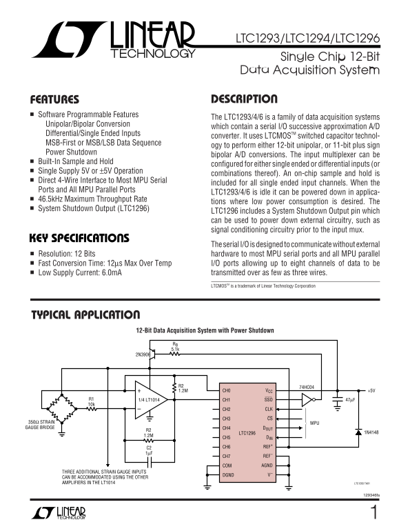
LTC1296 includes a System Shutdown Output pin which can be used to power down external circuitry, such as signal conditioning circuitry prior to the input mux.

KEY SPECIFICATIO S

The serial I/O is designed to communicate without external

Resolution: 12 Bits hardware to most MPU serial ports and all MPU parallel Fast Conversion Time: 12µs Max Over Temp I/O ports allowing up to eight channels of data to be

Low Supply Current: 6.0m A transmitted over as few as three wires. LTCMOSTM is a trademark of Linear Technology Corporation

PPLICATITYPICAL

12-Bit Data Acquisition System with Power Shutdown

RB 5.1k

R2 74HC04

1.2M CH0 VCC +5V

R1 1/4 LT1014 CH1 SSO 47µF 10k

CH2 CLK

CH3 CS

350Ω STRAIN MPU GAUGE BRIDGE CH4 DOUT

LTC1296 1N4148

CH5 DIN

C2 CH6 REF+

CH7 REF–

COM AGND

DGND V–THREE ADDITIONAL STRAIN GAUGE INPUTS

CAN BE ACCOMMODATED USING THE OTHER AMPLIFIERS IN THE LT1014 LTC1293 TA01

129346fs

Page Summary Contents For LINEAR TECHNOLOGY LTC1293, LTC1294, LTC1296 - Single Chip 12-Bit Data Acquisition System

Page 1 LTC1293/LTC1294/LTC1296 Single Chip 12-Bit Data Acquisition System ESCRIPTIOSFEATURE Software Programmable Features The LTC1293/4/6 is a family of data acquisition systems Unipolar/Bipolar Conversion ...
Page 2 LTC1293/LTC1294/LTC1296 XI ARBSOLUTE TI (Notes 1 and 2) Supply Voltage (VCC) to GND or V 12V Power Dissipation 500m W Negative Supply Voltage (V–) –6V to GND Operating Temperature Range Voltage LTC129...
Page 3 LTC1293/LTC1294/LTC1296 CO VERTER A D ULTIPLEXER CHARACTERISTICS (Note 3) LTC1293/4/6C LTC1293/4/6DLTC1293/4/6B PARAMETER CONDITIONS MIN TYP MAX MIN TYP MAX MIN TYP MAX UNITS Offset Error (Note 4) ±3....
Page 4 LTC1293/LTC1294/LTC1296 ELECTRICAL CHARA TER IDC STICSDIGITAL (Note 3) LTC1293/4/6B LTC1293/4/6C LTC1293/4/6D SYMBOL PARAMETER CONDITIONS MIN TYP MAX UNITS VIH High Level Input Voltage VCC = 5.25V 2.0...
Page 5 AG NI TU DE LI NE AR IT CH AN GE (L SB CH AN GE LI NE AR IT (L SB /4 EF SU PP LY UR RE NT (m A) LTC1293/LTC1294/LTC1296 PERFOR ATYPICAL CE CHARA TERISTICS Unadjusted Offset Voltage vs Supply Current v...
Page 6 OU RC (µ A) QU IS IT IO TI TO .0 2% (µ s) UT EL AY IM FR OM LK (n s) LTC1293/LTC1294/LTC1296 PERFOR ATYPICAL CE CHARA TERISTICS Maximum Clock Rate vs Source Maximum Filter Resistor vs Cycle Resistance...
Page 7 LTC1293/LTC1294/LTC1296 PI FU CTIO S LTC1293 PIN FUNCTION DESCRIPTION 1 – 6 CH0 – CH5 Analog Inputs The analog inputs must be free of noise with respect to AGND. COM Common The common pin defines the ...
Page 8 LTC1293/LTC1294/LTC1296 ID AGRABLOCK (Pin numbers refer to LTC1294) DVCC AVCC INPUT OUTPUT DIN SHIFT SHIFT DOUT REGISTER REGISTER SAMPLE CH1 AND HOLD CH2 COMP CH3 ANALOG INPUT MUX 12-BIT 12-BIT CH6 CA...
Page 9 LTC1293/LTC1294/LTC1296 TEST CIRCUITS Voltage Waveforms for ten START 0.8V B11DOUT LTC1293 TC07 Voltage Waveform for tdis SSO Voltage Waveform for DOUT Rise and Fall Times, tr, tf CS DOUT tdis SSO tr ...
Page 10 LTC1293/LTC1294/LTC1296 PPLICATI SA FOR ATIO The LTC 1293/4/6 is a data acquisition component which INPUT DATA WORD contains the following functional blocks: The LTC1293/4/6 seven-bit data word is clo...
Page 11 LTC1293/LTC1294/LTC1296 PPLICATI SA FOR ATIO REF –1LSB Table 1a. LTC1294/6 Multiplexer Channel Selection REF –2LSB MUX ADDRESS DIFFERENTIAL CHANNEL SELECTION MUX ADDRESS SINGLE-ENDED CHANNEL SELECTION...
Page 12 LTC1293/LTC1294/LTC1296 PPLICATI SA FOR ATIO Bipolar Transfer Curve (UNI = 0) INPUT VOLTAGE INPUT VOLTAGE OUTPUT CODE INPUT VOLTAGE (VREF = 5V) OUTPUT CODE INPUT VOLTAGE (VREF = 5V) REF –1LSB 0 1 1 1 ...
Page 13 LTC1293/LTC1294/LTC1296 PPLICATI SA FOR ATIO Example 2: The same conditions as Example 1 except MSB-First/LSB-First (MSBF) COM = 1V. The resulting input span is 1V ≤ IN+ ≤ 4V. Note The output data of ...
Page 14 LTC1293/LTC1294/LTC1296 PPLICATI SA FOR ATIO Power Shutdown Operating Sequence Example: Differential Inputs (CH4+, CH5–), Unipolar Mode and MSB-First Data CS NEW CONVERSION BEGINS SHUTDOWN*REQUEST POW...
Page 15 LTC1293/LTC1294/LTC1296 PPLICATI SA FOR ATIO Motorola SPI (MC68HC11) Interfacing to the Parallel Port of the Intel 8051 Family The MC68HC11 has been chosen as an example of an MPU The Intel 8051 has b...
Page 16 LTC1293/LTC1294/LTC1296 PPLICATI SA FOR ATIO MC68HC11 CODE LABEL MNEMONIC OPERAND COMMENTS LABEL MNEMONIC OPERAND COMMENTS LDAA #$50 CONFIGURATION DATA FOR SPCR STAA $102A LOAD DIN INTO SPI, START SCK...
Page 17 LTC1293/LTC1294/LTC1296 PPLICATI SA FOR ATIO 8051 CODE LABEL MNEMONIC OPERAND COMMENTS LABEL MNEMONIC OPERAND COMMENTS SETB P1.4 CS GOES HIGH CLR P1.3 CLK GOES LOW CONT MOV A,#87H DIN WORD FOR LTC1294...
Page 18 LTC1293/LTC1294/LTC1296 PPLICATI SA FOR ATIO LTC1294. Figure 4 shows an example of an ideal LTC1293/ 4/6 ground plane design for a two sided board. Of course this much ground plane will not always be ...
Page 19 LTC1293/LTC1294/LTC1296 PPLICATI SA FOR ATIO Source Resistance “–” Input Settling The analog inputs of the LTC1293/4/6 look like a 100p F At the end of the sample phase the input capacitor switches ca...
Page 20 LTC1293/LTC1294/LTC1296 PPLICATI SA FOR ATIO VE RT IC AL : 5 V/ DI VE RT IC AL : 5 V/ DI within the minimum settling windows of 2.5µs (“+” input) the cycle time as shown in the typical performance cha...
Page 21 LTC1293/LTC1294/LTC1296 PPLICATI SA FOR ATIO Usually VERROR will not be significant. For a 60Hz signal on the “–” input to generate a 0.25LSB error (300µV) with the converter running at CLK = 1MHz, it...
Page 22 LTC1293/LTC1294/LTC1296 PPLICATI SA FOR ATIO a 1.25 reference. If this offset is unacceptable, it can be example, with VREF = 1.25V this will result in a gain error corrected digitally by the receivin...
Page 23 LTC1293/LTC1294/LTC1296 AG NI TU DE (d B) AG NI TU DE (d B) EF FE CT IV NU BE OF IT PPLICATI SA FOR ATIO FREQUENCY (k Hz) FREQUENCY (k Hz) Figure 16a. LTC1294 FFT Plot Figure 18. LTC1294 FFT Plot f IN...
Page 24 LTC1293/LTC1294/LTC1296 PPLICATI SA FOR ATIO 1N4148 DIODES This means four channels can handle 7m A of input current each. Reducing CLK frequency from a maximum of 1MHz VCC +5V (See typical performanc...
Page 25 LTC1293/LTC1294/LTC1296 PPLICATI SA FOR ATIO A “Quick Look” Circuit for the LTC1294/6 Unipolar conversion is requested and the data is output Users can get a quick look at the function and timing of t...
Page 26 LTC1293/LTC1294/LTC1296 PPLICATITYPICAL SA Micropower, 5000V Opto-Isolated, Multichannel,12-Bit Data Acquisition System is Accessed Once Every Two Seconds LT1027 51k CH0 DVCC 5.1k CH1 AVCC C0 CH2 CLK ...
Page 27 LTC1293/LTC1294/LTC1296 PACKAGE DESCRIPTIO Dimensions in inches (millimeters) unless otherwise noted. J Package 20-Lead Ceramic DIP 0.290 - 0.320 MAX GLASS (4.064) SEALANT MAX MAX (5.588 - 7.874) (0.6...
Page 28 LTC1293/LTC1294/LTC1296 PACKAGE DESCRIPTIO Dimensions in inches (millimeters) unless otherwise noted. S Package 16-Lead Plastic SOL RAD MIN (2.362 – 2.642) 0° – 8° TYP 0.050 SEE NOTE 0.394 – 0.419 SEE...

Manual Details

Brand Linear
Pages 28
File Size 383.89 KB
Published June 21, 2026
12 views

Enter the captcha to get the download link:

captcha

Frequently Asked Questions

What are the operating temperature limits for different parts?

The LTC1293/4/6BC, CC, and DC can operate from 0°C to 70°C, while the -LTC1296 series (BI, CI, DI) offers wider range of –40°C to 85°C.

How does the LTC1296 power down external systems?

The LTC1296 includes a System Shutdown Output pin which can be used to power down external circuitry like signal conditioning prior to the input multiplexer.

What are the data acquisition system specifications?

It offers 12-bit resolution, up to 46.5kHz maximum throughput rate, and operates with low supply current.

Does the device support multiple types of inputs?

Yes, it supports both unipolar/bipolar conversion (12-bit unipolar or 11-bit plus sign bipolar) and can accommodate additional strain gauge inputs using other amplifiers like the LT1014.