# A B C D E F G H I J K L M N O P Q R S T U V W X Y Z

LINEAR TECHNOLOGY LTC1594L LTC1598L 4- and 8-Channel, 3V Micropower Sampling 12-Bit Serial I/O ADC Converters

Summary

The LTC1594L/LTC1598L are advanced 12-bit, micropower Analog-to-Digital Converters featuring automated multiplexing for 4- and 8-channel data acquisition. Designed to operate efficiently on a low 3V supply, these converters minimize power consumption in demanding environments. The manual serves as a comprehensive technical guide for engineers needing reliable, battery-operated sensing solutions, covering detailed electrical specifications, multiple serial I/O protocols (SPI, QSPI), and optimal implementation strategies for remote monitoring and data isolation.
📄 Preview PAGE OF 24

Page 1 Text Content

LTC1594L/LTC1598L 4- and 8-Channel,

3V Micropower Sampling 12-Bit Serial I/O A/D Converters

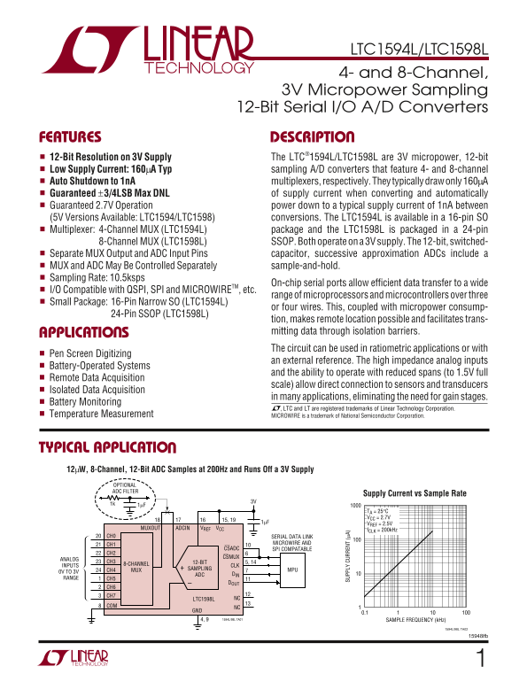
FEATURES DESCRIPTIO 12-Bit Resolution on 3V Supply The LTC®1594L/LTC1598L are 3V micropower, 12-bit Low Supply Current: 160µA Typ sampling A/D converters that feature 4- and 8-channel Auto Shutdown to 1n A multiplexers, respectively. They typically draw only 160µA

Guaranteed ±3/4LSB Max DNL of supply current when converting and automatically Guaranteed 2.7V Operation power down to a typical supply current of 1n A between (5V Versions Available: LTC1594/LTC1598) conversions. The LTC1594L is available in a 16-pin SO Multiplexer: 4-Channel MUX (LTC1594L) package and the LTC1598L is packaged in a 24-pin 8-Channel MUX (LTC1598L) SSOP. Both operate on a 3V supply. The 12-bit, switched- Separate MUX Output and ADC Input Pins capacitor, successive approximation ADCs include a MUX and ADC May Be Controlled Separately sample-and-hold.

Sampling Rate: 10.5ksps

On-chip serial ports allow efficient data transfer to a wide

I/O Compatible with QSPI, SPI and MICROWIRETM, etc.

range of microprocessors and microcontrollers over three

Small Package: 16-Pin Narrow SO (LTC1594L)

or four wires. This, coupled with micropower consump-

24-Pin SSOP (LTC1598L)

tion, makes remote location possible and facilitates trans- APPLICATIO S mitting data through isolation barriers.

SU PP LY UR RE NT (µ A) The circuit can be used in ratiometric applications or with

Pen Screen Digitizing

an external reference. The high impedance analog inputs

Battery-Operated Systems

and the ability to operate with reduced spans (to 1.5V full

Remote Data Acquisition

scale) allow direct connection to sensors and transducers

Isolated Data Acquisition

in many applications, eliminating the need for gain stages.

Battery Monitoring

, LTC and LT are registered trademarks of Linear Technology Corporation.

Temperature Measurement MICROWIRE is a trademark of National Semiconductor Corporation.

TYPICAL APPLICATION 12µW, 8-Channel, 12-Bit ADC Samples at 200Hz and Runs Off a 3V Supply

OPTIONAL ADC FILTER

Supply Current vs Sample Rate

TA = 25°C VCC = 2.7V

1µF VREF = 2.5V

MUXOUT ADCIN VREF VCC

f CLK = 200k Hz

CH0 SERIAL DATA LINK

CH1 MICROWIRE AND

CSADC SPI COMPATABLE

CSMUX

ANALOG

CH3 12-BIT 5, 14 INPUTS 8-CHANNEL CLK

CH4 MUX SAMPLING MPU

0V TO 3V

ADC DIN

RANGE CH5

CH6 CH7

LTC1598L NC

COM NC

4, 9 1594L/98L TA01 SAMPLE FREQUENCY (k Hz)

1594L/98L TA02

15948lfb

Page Summary Contents For LINEAR TECHNOLOGY LTC1594L LTC1598L 4- and 8-Channel, 3V Micropower Sampling 12-Bit Serial I/O ADC Converters

Page 1 LTC1594L/LTC1598L 4- and 8-Channel, 3V Micropower Sampling 12-Bit Serial I/O A/D Converters FEATURES DESCRIPTIO 12-Bit Resolution on 3V Supply The LTC®1594L/LTC1598L are 3V micropower, 12-bit Low Supp...
Page 2 LTC1594L/LTC1598L ABSOLUTE MAXIMUM RATINGS (Notes 1, 2) Supply Voltage (VCC) to GND................................... 12V Power Dissipation 500m W Voltage Operating Temperature Range Analog Reference...
Page 3 LTC1594L/LTC1598L CONVERTER AND MULTIPLEXER CHARACTERISTICS The ● denotes the specifications which apply over the full operating temperature range, otherwise specifications are at TA = 25°C. (Note 5) ...
Page 4 SU PP LY UR RE NT (µ A) LTC1594L/LTC1598L AC CHARACTERISTICS The ● denotes the specifications which apply over the full operating temperature range, otherwise specifications are at TA = 25°C.(Note 5) ...
Page 5 SP UR IO US -F RE DY NA IC AN GE (d B) CH AN S/(N + D) (d B) GE IN AI (L SB CH AN GE IN FF SE (L SB /4 LTC1594L/LTC1598L TYPICAL PERFORMANCE CHARACTERISTICS Change in Offset Change in Linearity vs Ref...
Page 6 AG NI TU DE (d B) LTC1594L/LTC1598L TYPICAL PERFORMANCE CHARACTERISTICS Power Supply Feedthrough CL OC FR EQ UE NC (k Hz CL OC FR EQ UE NC (k Hz 4096 Point FFT Plot Intermodulation Distortion vs Rippl...
Page 7 LTC1594L/LTC1598L PIN FUNCTIONS LTC1594L CH0 (Pin 1): Analog Multiplexer Input. DOUT (Pin 10): Digital Data Output. The A/D conversion result is shifted out of this output. CH1 (Pin 2): Analog Multipl...
Page 8 LTC1594L/LTC1598L PIN FUNCTIONS VCC (Pin 15): Power Supply Voltage. This pin provides VCC (Pin 19): Power Supply Voltage. This pin should be power to the A/D Converter. It must be bypassed directly ti...
Page 9 LTC1594L/LTC1598L TEST CIRCUITS Voltage Waveforms for ten Voltage Waveforms for DOUT Delay Times, td DO LTC1594L/LTC1598L CLK CSADC td DO 1594L/98L TC03 1594L/98L TC06 Load Circuit for tdis and ten Vo...
Page 10 LTC1594L/LTC1598L APPLICATIONS INFORMATION OVERVIEW and can operate with reduced spans to 1.5V. Reducing the spans allow them to achieve 366µV resolution. The LTC1594L/LTC1598L are 3V micropower, 12-b...
Page 11 LTC1594L/LTC1598L APPLICATIONS INFORMATION t CYC CSMUX = CSADC = CS tsu CS EN D1 DIN D0N‘T CARE Hi-Z BIT Hi-ZDOUT DUMMY CONVERSION t CONV CH0 TO CH7 t OFF ADCIN = MUXOUT COM = GND Figure 2. LTC1594L/L...
Page 12 LTC1594L/LTC1598L REF –1LSB APPLICATIONS INFORMATION REF –2LSB after a delay of t OFF, all the channels are switched off to Table 2. Logic Table for the LTC1598L Channel Selection ensure a break-befor...
Page 13 LTC1594L/LTC1598L APPLICATIONS INFORMATION Operation with DIN and DOUT Tied Together (see Figure 3). Therefore the processor port line must be switched to an input with CS being low to avoid a conflic...
Page 14 LTC1594L/LTC1598L APPLICATIONS INFORMATION CSADC CSMUX tsu CS tsu CS EN D1 EN D1 EN D1 DIN DON’T CARE DON’T CARE NULL NULL BIT BIT B4 B3 B2 B1 B0 B5B6B7B8B9B10B11DOUT B4 B3 B2 B1 B0 B5B6B7B8B9B10B11 B...
Page 15 LTC1594L/LTC1598L APPLICATIONS INFORMATION BOARD LAYOUT CONSIDERATIONS SAMPLE-AND-HOLD Both the LTC1594L/LTC1598L provide a built-in sample- Grounding and Bypassing and-hold (S&H) function to acqu...
Page 16 LTC1594L/LTC1598L APPLICATIONS INFORMATION edge, the S & H goes into hold mode and the conversion “COM” Input Settling begins. The voltage on the “COM” input must remain At the end of the t SMPL, ...
Page 17 LTC1594L/LTC1598L APPLICATIONS INFORMATION Input Leakage Current Offset with Reduced VREF Input leakage currents can also create errors if the source The offset of the LTC1594L/LTC1598L has a larger e...
Page 18 LTC1594L/LTC1598L AG NI TU DE (d B) APPLICATIONS INFORMATION Conversion Speed with Reduced VREF Effective Number of Bits With reduced reference voltages, the LSB step size is The Effective Number of B...
Page 19 LTC1594L/LTC1598L APPLICATIONS INFORMATION specification in the Dynamic Accuracy table includes the mplitude ±( ) 2nd through 5th harmonics. With a 1k Hz input signal, the IMD ±( 20log LTC1594L/LTC15...
Page 20 LTC1594L/LTC1598L TYPICAL APPLICATIONS N MC68HC05 CODE LDA #$52 Configuration data for serial peripheral BPL LOOP1 Loop if not done with transfer to previous instruction control register (Interrupts d...
Page 21 LTC1594L/LTC1598L TYPICAL APPLICATIONS N MULTICHANNEL A/D USES A SINGLE than 1LSB of error due to offsets and bias currents. The ANTIALIASING FILTER filter’s noise and distortion are less than –72d B ...
Page 22 LTC1594L/LTC1598L TYPICAL APPLICATIONS N Using MUXOUT/ADCIN Loop as PGA the summation of the resistors below the selected MUX channel. If CH0 is selected, the gain is 1 since RS1 is 0. This figure sho...
Page 23 LTC1594L/LTC1598L PACKAGE DESCRIPTION G Package 24-Lead Plastic SSOP (0.209) (LTC DWG # 05-08-1640) NOTE: 0.42 ±0.03 0.65 BSC 1. CONTROLLING DIMENSION: MILLIMETERS RECOMMENDED SOLDER PAD LAYOUT MILLIM...
Page 24 LTC1594L/LTC1598L TYPICAL APPLICATION Using the LTC1598L and LTC1391 as an 8-Channel Differential 12-Bit ADC System ADCINMUXOUT VREF VCC CH0 CH1 CSADC CSMUX CH3 12-BIT 5, 14 8-CHANNEL 1µF CH4 MUX SAMP...

Manual Details

Brand Linear
Pages 24
File Size 354.44 KB
Published June 05, 2026
57 views

Enter the captcha to get the download link:

captcha

Frequently Asked Questions

What is the power consumption?

The converters typically draw only 160μA and can enter a low current state of 1nA.

How many channels are available in the LTC1598L?

The LTC1598L is an 8-Channel MUX configured for 12-Bit serial I/O.

What types of data interfaces are compatible with these converters?

They support QSPI, SPI, and MICROWIRE, facilitating efficient data transfer to microprocessors.

Does this system require external gain stages?

No, the high impedance analog inputs allow for direct connection to sensors, eliminating the need for gain stages.