LINEAR TECHNOLOGY LTC1154 Specification Sheet User Guide
Summary
The LTC1154 is a micropower high-side gate driver designed to efficiently switch N-channel MOSFETs in power applications. Featuring internal charge pumping, it requires no external charge pump components. The manual details its robust features, including integrated short-circuit protection and thermal shutdown capabilities with status output monitoring. This versatile IC is ideal for engineers developing battery charging systems, stepper/DC motor control, or complex industrial and automotive switch management requiring low standby current consumption.
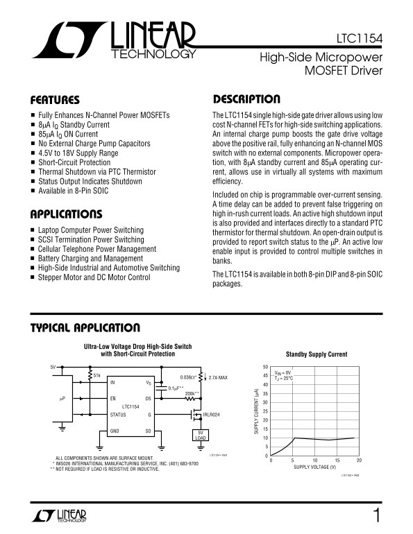
Page 1 Text Content
LTC1154
High-Side Micropower MOSFET Driver
ESCRIPTIOSFEATURE
Fully Enhances N-Channel Power MOSFETs The LTC1154 single high-side gate driver allows using low
8µA IQ Standby Current cost N-channel FETs for high-side switching applications. 85µA IQ ON Current An internal charge pump boosts the gate drive voltage
No External Charge Pump Capacitors above the positive rail, fully enhancing an N-channel MOS
4.5V to 18V Supply Range switch with no external components. Micropower opera- Short-Circuit Protection tion, with 8µA standby current and 85µA operating cur- Thermal Shutdown via PTC Thermistor rent, allows use in virtually all systems with maximum Status Output Indicates Shutdown efficiency.
Available in 8-Pin SOIC
Included on chip is programmable over-current sensing. A time delay can be added to prevent false triggering on PPLICATI SA high in-rush current loads. An active high shutdown input is also provided and interfaces directly to a standard PTC
Laptop Computer Power Switching
thermistor for thermal shutdown. An open-drain output is
SCSI Termination Power Switching
provided to report switch status to the µP. An active low
Cellular Telephone Power Management
enable input is provided to control multiple switches in
SU PP LY UR RE NT (µ A)
Battery Charging and Management
banks.
High-Side Industrial and Automotive Switching
The LTC1154 is available in both 8-pin DIP and 8-pin SOIC
Stepper Motor and DC Motor Control
packages.
PPLICATITYPICAL Ultra-Low Voltage Drop High-Side Switch with Short-Circuit Protection Standby Supply Current 5V
VIN = 0V
0.036Ω* 2.7A MAX51k TJ = 25°C
IN VS
µP EN DS
LTC1154
STATUS IRLR024
GND SD
5V LOAD
LTC1154 • TA01
ALL COMPONENTS SHOWN ARE SURFACE MOUNT. IMS026 INTERNATIONAL MANUFACTURING SERVICE, INC. (401) 683-9700
SUPPLY VOLTAGE (V)
NOT REQUIRED IF LOAD IS RESISTIVE OR INDUCTIVE.
LTC1153 • TA02
Page Summary Contents For LINEAR TECHNOLOGY LTC1154 Specification Sheet User Guide
Manual Details
| Brand | Linear |
|---|---|
| Pages | 16 |
| File Size | 278.27 KB |
| Published | June 17, 2026 |
Enter the captcha to get the download link:

Frequently Asked Questions
What is the required supply voltage range for operation?
The LTC1154 operates with a supply range of 4.5V to 18V.
Does this device offer protection against overcurrent and thermal issues?
Yes, it includes Short-Circuit Protection, Thermal Shutdown via PTC Thermistor, and programmable over-current sensing.
How can the status of the switch be monitored by a microcontroller?
Status is reported to the μP using an open-drain output (SD) for interface with SCSI Termination. Alternatively, there is a dedicated active low enable input (EN).
Are there any external components required for basic operation?
No external charge pump capacitors are needed above the positive rail; the device fully enhances the MOSFET without extra components.