# A B C D E F G H I J K L M N O P Q R S T U V W X Y Z

LINEAR TECHNOLOGY LTC1091 LTC1092 LTC1093 LTC1094 User Manual

Summary

These high-precision 10-Bit Serial I/O Data Acquisition Systems are versatile sample-and-hold units designed for complex analog data collection. The manual details their ability to provide up to eight channels of multi-mode acquisition, supporting both unipolar and bipolar conversions directly from sensors or transceivers. Ideal for sophisticated microprocessors and industrial applications, these ADCs feature extremely low power consumption and minimal error rates (–1LSB max). They deliver reliable, multichannel signal interfacing with streamlined connections, making them perfect for remote monitoring and demanding automation systems.
📄 Preview PAGE OF 32

Page 1 Text Content

LTC1091/LTC1092 LTC1093/LTC1094

1-, 2-, 6- and 8-Channel, 10-Bit Serial I/O Data Acquisition Systems

FEATURES and-holds. On-chip serial ports allow efficient data trans- fer to a wide range of microprocessors and microcontrol-

Programmable Features

lers. These circuits can provide a complete data acquisi-

Unipolar/Bipolar Conversions

tion system in ratiometric applications or can be used with

Differential/Single-Ended Multiplexer

an external reference in others.

Configurations

The high impedance analog inputs and the ability to

Sample-and-Holds

operate with reduced spans (below 1V full scale) allow

Single Supply 5V, 10V or ±5V Operation

direct connection to sensors and transducers in many

Direct 3- or 4-Wire Interface to Most MPU Serial

applications, eliminating the need for gain stages.

Ports and All MPU Parallel I/O Ports Analog Inputs Common Mode to Supply Rails An efficient serial port communicates without external Resolution: 10 Bits hardware to most MPU serial ports and all MPU parallel Total Unadjusted Error (A Grade): ±1LSB Over Temp I/O ports allowing eight channels of data to be transmitted Fast Conversion Time: 20µs over as few as three wires. This, coupled with low power Low Supply Current consumption, makes remote location possible and facili- LTC1091: 3.5m A Max, 1.5m A Typ tates transmitting data through isolation barriers. LTC1092/LTC1093/LTC1094: 2.5m A Max, 1m A Typ

Temperature drift of offset, linearity and full-scale error

LI NE AR IT ER RO (L SB • V RE F)

are all extremely low (1ppm/°C typically) allowing all DESCRIPTIO grades to be specified with offset and linearity errors of ±0.5LSB maximum over temperature. In addition, the A

The LTC®1091/LTC1092/LTC1093/LTC1094 10-bit data

grade devices are specified with full-scale error and total

acquisition systems are designed to provide complete

unadjusted error (including the effects of offset, linearity

function, excellent accuracy and ease of use when digitiz-

and full-scale errors) of ±1LSB maximum over tempera-

ing analog data from a wide variety of signal sources and

ture. The lower grade has a full-scale specification of

transducers. Built around a 10-bit, switched capacitor,

±2LSB for applications where full scale is adjustable or

successive approximation A/D core, these devices include

less critical.

software configurable analog multiplexers and bipolar and

unipolar conversion modes as well as on-chip sample- , LTC and LT are registered trademarks of Linear Technology Corporation.

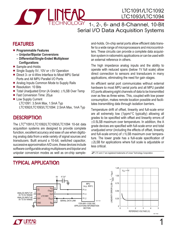
TYPICAL APPLICATION

1.25 VCC = 5V

MPU 0.75

CS P1.4

(VREF) 0.50

ANALOG INPUT #1

CH0 CLK P1.3

0V TO 5V RANGE

LTC1091

ANALOG INPUT #2

CH1 DOUT P1.2 0.25

0V TO 5V RANGE

SERIAL DATA LINK 1091 TA01

GND DIN

FOR 8051 CODE SEE APPLICATIONS INFORMATION SECTION

REFERENCE VOLTAGE (V)

1091 TA02

Page Summary Contents For LINEAR TECHNOLOGY LTC1091 LTC1092 LTC1093 LTC1094 User Manual

Page 1 LTC1091/LTC1092 LTC1093/LTC1094 1-, 2-, 6- and 8-Channel, 10-Bit Serial I/O Data Acquisition Systems FEATURES and-holds. On-chip serial ports allow efficient data trans- fer to a wide range of micropr...
Page 2 LTC1091/LTC1092 LTC1093/LTC1094 XI ARBSOLUTE TI (Notes 1, 2) Supply Voltage (VCC) to GND or V 12V Power Dissipation 500m W Negative Supply Voltage (V –6V to GND Operating Temperature Range Voltage LTC...
Page 3 LTC1091/LTC1092 LTC1093/LTC1094 RECO E DED OPERATI G CO DITIO S LTC1091A/LTC1092A/LTC1093A/LTC1094A LTC1091/LTC1092/LTC1093/LTC1094 SYMBOL PARAMETER CONDITIONS MIN MAX UNITS VCC Supply Voltage 4.5 V– ...
Page 4 LTC1091/LTC1092 LTC1093/LTC1094 AC CHARACTERISTICS The ● denotes specifications which apply over the full operating temperature range, otherwise specifications are TA = 25°C. (Note 3) LTC1091A/LTC1092...
Page 5 LTC1091/LTC1092 AX IM UM LK RE QU EN CY (M Hz LO GI TH RE SH OL (V AG NI TU DE OF FS ET HA NG (L SB LTC1093/LTC1094 PERFOR ATYPICAL CE CHARA TERISTICS Change in Offset Error vs Change in Linearity Err...
Page 6 LTC1091/LTC1092 CH AN GE IN UL L- SC AL ER RO IN PU CH AN NE LE AK AG CU RR EN (n A) AX IM UM LK RE QU EN CY (M Hz LTC1093/LTC1094 [L SB • V CC (V RE F) PERFOR ATYPICAL CE CHARA TERISTICS LTC1091/LTC1...
Page 7 LTC1091/LTC1092 CH AN GE IN UL L- SC AL ER RO (L SB PE AK -T O- PE AK OI SE RR OR (L SB OF FS ET RR OR (L SB • V RE F) LTC1093/LTC1094 PERFOR ATYPICAL CE CHARA TERISTICS LTC1092/LTC1093/LTC1094 LTC109...
Page 8 LTC1091/LTC1092 LTC1093/LTC1094 PERFOR ATYPICAL CE CHARA TERISTICS RE FE RE NC CU RR EN (m A) LTC1092/LTC1093/LTC1094 LTC1093/LTC1094 Input Channel Reference Current vs Temperature Leakage Current vs ...
Page 9 LTC1091/LTC1092 LTC1093/LTC1094 PI FU CTIO S VREF (Pin 11)(LTC1093): Reference Input. The reference CLK (Pin 15/Pin 18): Shift Clock. This clock synchronizes input must be kept free of noise with resp...
Page 10 LTC1091/LTC1092 LTC1093/LTC1094 TEST CIRCUITS On- and Off-Channel Leakage Current Load Circuit for td DO, t ON-CHANNEL DOUT TEST POINT OFF- CHANNELS 1091/2/3/4 TC02 POLARITY 1091/2/3/4 TC01 Voltage Wa...
Page 11 LTC1091/LTC1092 LTC1093/LTC1094 TEST CIRCUITS Voltage Waveforms for ten LTC1092 1091/2/3/4 TC08 LTC1093/LTC1094 DIN START B9DOUT 1091/2/3/4 TC09 PPLICATI SA FOR ATIO The LTC1091/LTC1092/LTC1093/LTC109...
Page 12 LTC1091/LTC1092 LTC1093/LTC1094 PPLICATI SA FOR ATIO CS sequence, providing easy interface to MSB- or LSB-first serial ports. The following disussion applies to the con- DIN 1 DIN 2 figuration of the ...
Page 13 LTC1091/LTC1092 LTC1093/LTC1094 PPLICATI SA FOR ATIO LTC1092 Operating Sequence t CYC Hi-Z DOUT B1B9 B1 B9B0 t SMPL t CONV t SMPL 1091/2/3/4 AI05 LTC1093/LTC1094 Operating Sequence Example: Differenti...
Page 14 LTC1091/LTC1092 LTC1093/LTC1094 PPLICATI SA FOR ATIO Start Bit voltage between the two channels indicated by the + and – signs in the selected row of the following tables. In The first “logical one” c...
Page 15 LTC1091/LTC1092 LTC1093/LTC1094 PPLICATI SA FOR ATIO MSB-First/LSB-First (MSBF) Unipolar Output Code (UNI = 1) INPUT VOLTAGE The output data of the LTC1091/LTC1093/LTC1094 is OUTPUT CODE INPUT VOLTAGE...
Page 16 LTC1091/LTC1092 LTC1093/LTC1094 PPLICATI SA FOR ATIO 3. Accommodating Microprocessors with eliminates one 8-bit transfer and positions data right Different Word Lengths justified inside the MPU. The L...
Page 17 LTC1091/LTC1092 LTC1093/LTC1094 PPLICATI SA FOR ATIO MSBF LATCHED BY LTC1091 SGL/ ODD/ DATA (DIN/DOUT) START MSBF B9 B8 • • • DIFF SIGN MPU CONTROLS LTC1091 CONTROLS DATA LINE AND SENDS DATA LINE AND ...
Page 18 LTC1091/LTC1092 LTC1093/LTC1094 PPLICATI SA FOR ATIO Motorola SPI (MC68HC05C4, MC68HC11) second 8-bit transfer clocks the remaining bits, B7 through B0, into the MPU. The MC68HC05C4 has been chosen as...
Page 19 LTC1091/LTC1092 LTC1093/LTC1094 PPLICATI SA FOR ATIO Interfacing to the Parallel Port of the LABEL MNEMONIC OPERAND COMMENTS Intel 8051 Family MOV A, #FFH DIN Word for LTC1091 SETB P1.4 Make Sure CS I...
Page 20 LTC1091/LTC1092 LTC1093/LTC1094 PPLICATI SA FOR ATIO OUTPUT PORT 3-WIRE SERIAL SERIAL DATA INTERFACE TO OTHER PERIPHERALS OR LTC1094s CS CS CS LTC1094 LTC1094 LTC1094 LTC1091-4 F03 8 CHANNELS 8 CHANNE...
Page 21 LTC1091/LTC1092 LTC1093/LTC1094 PPLICATI SA FOR ATIO 3. Analog Inputs Because of the capacitive redistribution A/D conversion techniques used, the analog inputs of the LTC1091/ LTC1092/LTC1093/LTC1094...
Page 22 LTC1091/LTC1092 LTC1093/LTC1094 PPLICATI SA FOR ATIO “–” Input Settling Input Op Amps At the end of the sample phase the input capacitor switches When driving the analog inputs with an op amp it is to...
Page 23 LTC1091/LTC1092 LTC1093/LTC1094 PPLICATI SA FOR ATIO resistor must be used, errors can be eliminated by increas- ing the cycle time as shown in the typical curve of Maximum Filter Resistor vs Cycle Ti...
Page 24 LTC1091/LTC1092 LTC1093/LTC1094 PPLICATI SA FOR ATIO Differential Inputs 2. Transients on the reference inputs caused by the With differential inputs, the A/D no longer converts just a capacitive swit...
Page 25 LTC1091/LTC1092 LTC1093/LTC1094 PPLICATI SA FOR ATIO 5V reference becomes 0.5LSB with a 1V reference and 2.5LSBs with a 0.2V reference. If this offset is unaccept- able, it can be corrected digitally ...
Page 26 LTC1091/LTC1092 LTC1093/LTC1094 PPLICATITYPICAL SA 0°C to 500°C Furnace Exhaust Gas Temperature Monitor with Low Supply Detection 9V VIN VOUT LT1021-5 56k VIN 10µF J– LT1025A 20k GNDJ TYPE COMMON LTC1...
Page 27 LTC1091/LTC1092 LTC1093/LTC1094 PPLICATITYPICAL SA 0°C to 100°C 0.25°C Accurate Thermistor Based Temperature Measurement System LTC1094 YSI 44201 CH0 DVCC CH1 AVCC 0°C TO 100°C CH2 CLK CH3 CS TO 5k AT...
Page 28 LTC1091/LTC1092 LTC1093/LTC1094 PACKAGE DESCRIPTIO Dimensions in inches (millimeters) unless otherwise noted. N8 Package 8-Lead PDIP (Narrow 0.300) (LTC DWG # 05-08-1510) 0.400* (10.160) MAX 0.065 (1....
Page 29 LTC1091/LTC1092 LTC1093/LTC1094 PACKAGE DESCRIPTIO Dimensions in inches (millimeters) unless otherwise noted. N Package 16-Lead PDIP (Narrow 0.300) (LTC DWG # 05-08-1510) 0.770* (19.558) MAX 0.020 (0....
Page 30 LTC1091/LTC1092 LTC1093/LTC1094 PACKAGE DESCRIPTIO Dimensions in inches (millimeters) unless otherwise noted. N Package 20-Lead PDIP (Narrow 0.300) (LTC DWG # 05-08-1510) 1.040* (26.416) MAX MIN 0.065...
Page 31 LTC1091/LTC1092 LTC1093/LTC1094 PACKAGE DESCRIPTIO Dimensions in inches (millimeters) unless otherwise noted. SW Package 16-Lead Plastic Small Outline (Wide 0.300) (LTC DWG # 05-08-1620) NOTE 1 0.394 ...
Page 32 LTC1091/LTC1092 LTC1093/LTC1094 TYPICAL APPLICATION Micropower, 500V Optoisolated, Multichannel, 10-Bit Data Acquisition System Is Accessed Once Every Two Seconds LT1021-5 51k LTC1094 CH0 DVCC 5.1k CH...

Manual Details

Brand Linear
Pages 32
File Size 276.85 KB
Published June 17, 2026
3 views

Enter the captcha to get the download link:

captcha

Frequently Asked Questions

What is the maximum resolution and typical error for these data acquisition systems?

The devices offer a 10-bit resolution, with a total unadjusted error of -1 LSB (A Grade) or -2 LSB for less critical applications.

Can the device operate directly from external sensors without complex circuitry?

Yes, because of the high impedance analog inputs and ability to Sample-and-Hold, it allows direct connection to sensors in many applications, eliminating the need for gain stages.

What is the typical maximum operating temperature range?

The LTC1091/2/3/4 devices operate from -40°C to 85°C. The analog reference and storage temperatures are wider, ranging from -65°C to 150°C.

How much current do these channels consume at typical operating points?

For the LTC1091 (A Grade), the maximum supply current is 3.5mA (typical: 1.5mA). For LTC1092/LTC1093/LTC1094, it is 2.5mA Max (typical: 1mA).

Are there options for differential or bipolar measurements?

Yes, the circuits can accommodate both Unipolar/Bipolar Conversions and Differential/Single-Ended Multiplexer configurations.