Linear Design Features LTMag-V18N03-10-LT3513 - Kevin Huang Owner's Manual Technical Guide
Summary
This highly integrated multi-output DC-DC regulator provides a complete power solution for sensitive electronics. The device delivers five tightly controlled voltages from a wide input range (e.g., 8V to 30V), featuring step-down and boost capabilities to maximize efficiency while minimizing board space. It is ideal for designers building advanced, compact systems like large TFT-LCD displays or portable industrial equipment that require multiple stable power rails and high reliability in a low-profile QFN package.
Page 1 Text Content
L DESIGN IDEAS
5-Output High Current Power Supply for TFT-LCDs in a Low Profile QFN Features Space-Saving 2MHz Switching Regulators by Kevin Huang
Introduction L1 DFLS240L 10µH
VIN VLOGIC
The LT3513 is a highly integrated, 8V TO 30V 5V
5-output regulator designed to pro- ZHCS400 0.47µF
VOFF Si2333DS vide all the supply voltages typically –10V
L2 UVLO LDOPWR VIN SW2
required by large TFT liquid crystal 2.2µF AVDD
10µH SW4 FB2
displays (LCDs) with a single IC. The 80m A
69.8k D4 PGOOD
part features a step-down switching NFB4 RUN-SS1
10k BIAS RUN-SS2
regulator to produce a 3.3V or 5V
BOOST RUN-SS3/4
logic voltage from a wide voltage range 0.22µF
4.7µH CT
VLOGIC SW1 47n F 15n F 15n F 15n F
input, such as automotive battery.
5V LT3513
SENSE+
A lower voltage logic supply can be 0.5A
30.1k VON_CLK VON_CLK
SENSE– VON
generated from the first supply by 22µF FB1 VON 22V
10k DFLS240L VONSINK
adding an external NPN driven by an
internal linear regulator. The other 165k
ZXTAM322 6.8µH
VLOGIC
BD SW3
three on-chip regulators provide the VLDO 5V
FB5 FB3 0.47µF
three bias voltages required by LCDs: a 0.5A
VC1 VC2 GND VC3 VC4
high power boost regulator to generate
AVDD, a low power boost regulator to 10k
generate VON and an inverting regula-
L1: SUMIDA CDR6D28MNNP-100NC L2: COILCRAFT LPO3310-103MLC
tor to provide VOFF.
L3: SUMIDA CDR6D28MNNP-4R5NC L4: COILCRAFT LPO3310-682MLC
Switching regulators are chosen
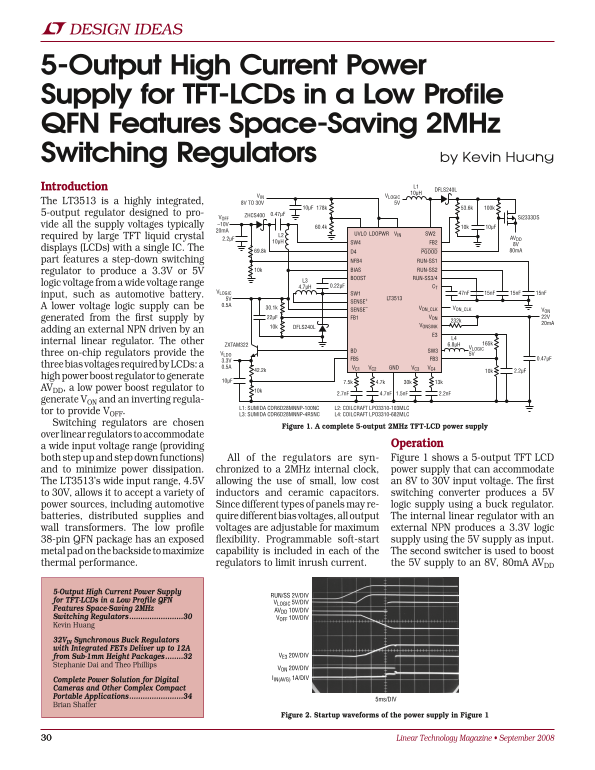
Figure 1. A complete 5-output 2MHz TFT-LCD power supply
over linear regulators to accommodate
a wide input voltage range (providing Operation
both step up and step down functions) All of the regulators are syn- Figure 1 shows a 5-output TFT LCD and to minimize power dissipation. chronized to a 2MHz internal clock, power supply that can accommodate The LT3513’s wide input range, 4.5V allowing the use of small, low cost an 8V to 30V input voltage. The first to 30V, allows it to accept a variety of inductors and ceramic capacitors. switching converter produces a 5V power sources, including automotive Since different types of panels may re- logic supply using a buck regulator. batteries, distributed supplies and quire different bias voltages, all output The internal linear regulator with an wall transformers. The low profile voltages are adjustable for maximum external NPN produces a 3.3V logic 38-pin QFN package has an exposed flexibility. Programmable soft-start supply using the 5V supply as input. metal pad on the backside to maximize capability is included in each of the The second switcher is used to boost thermal performance. regulators to limit inrush current. the 5V supply to an 8V, 80m A AVDD
5-Output High Current Power Supply
RUN/SS 2V/DIV
for TFT-LCDs in a Low Profile QFN VLOGIC 5V/DIV Features Space-Saving 2MHz AVDD 10V/DIV Switching Regulators ........................30 VOFF 10V/DIV Kevin Huang
32VIN Synchronous Buck Regulators with Integrated FETs Deliver up to 12A
from Sub-1mm Height Packages ........32 VE3 20V/DIV
Stephanie Dai and Theo Phillips
VON 20V/DIV IIN(AVG) 1A/DIV
Complete Power Solution for Digital Cameras and Other Complex Compact Portable Applications ........................34
5ms/DIV
Brian Shaffer
Figure 2. Startup waveforms of the power supply in Figure 1
Linear Technology Magazine • September 2008
Page Summary Contents For Linear Design Features LTMag-V18N03-10-LT3513 - Kevin Huang Owner's Manual Technical Guide
Manual Details
| Brand | Linear |
|---|---|
| Pages | 2 |
| File Size | 377.40 KB |
| Published | June 20, 2026 |
Enter the captcha to get the download link:

Frequently Asked Questions
What overall voltage range can the LT3513 regulate?
It is designed to operate from an input voltage of 8V up to 30V.
How does the LT3513 power LCDs?
It uses three on-chip regulators to provide the required bias voltages for LCDs: 3.3V, 5V, and an adjustable 8V boost supply.
Is external component mounting flexible with this device?
Yes, it features a 38-pin QFN package with an exposed metal pad on the backside to maximize thermal performance and simplify layout designs.
What is the characteristic of switching regulators used in the LT3513?
They are synchronized to a 2MHz internal clock operation, which minimizes power dissipation.