LINEAR Circuit Techniques for Clock Sources Data Sheet 12
Summary
Optimize your circuit design with this application note on stable clock source techniques. Learn proven best practices for integrating quartz crystals and building reliable oscillator circuits using various gate types (CMOS, TTL). Coverage includes component selection, minimizing temperature drift, and ensuring precise frequency stability necessary for demanding digital and communication systems. Essential reading for electrical engineers designing high-accuracy timing equipment.
Page 1 Text Content
Application Note 12
October 1985
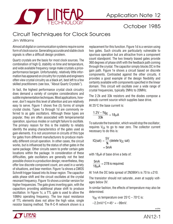
Circuit Techniques for Clock Sources Jim Williams Almost all digital or communication systems require some replacement for this function. Figure 1d is a version using form of clock source. Generating accurate and stable clock two gates. Such circuits are particularly vulnerable to signals is often a difficult design problem. spurious operation but are attractive from a component
count standpoint. The two linearly biased gates provide
Quartz crystals are the basis for most clock sources. The
360 degrees of phase shift with the feedback path coming
combination of high Q, stability vs time and temperature,
through the crystal. The capacitor simply blocks DC in the
and wide available frequency range make crystals a price-
gain path. Figure 1e shows a circuit based on discrete
performance bargain. Unfortunately, relatively little infor-
components. Contrasted against the other circuits, it
mation has appeared on circuitry for crystals and engineers
provides a good example of the design flexibility and
often view crystal circuitry as a black art, best left to a few
certainty available with components specified in the linear
skilled practitioners (see box, “About Quartz Crystals”).
domain. This circuit will oscillate over a wide range of
In fact, the highest performance crystal clock circuitry crystal frequencies, typically 2MHz to 20MHz. does demand a variety of complex considerations and
The 2.2k and 33k resistors and the diodes compose a
subtle implementation techniques. Most applications, how-
pseudo current source which supplies base drive.
ever, don’t require this level of attention and are relatively easy to serve. Figure 1 shows five (5) forms of simple At 25°C the base current is: crystal clocks. Types 1a through 1d are commonly re-
ferred to as gate oscillators. Although these types are –V
popular, they are often associated with temperamental operation, spurious modes or outright failure to oscillate.
To saturate the transistor, which would stop the oscillator,
The primary reason for this is the inability to reliably
requires VCE to go to near zero. The collector current
identify the analog characteristics of the gates used as
necessary to do this is:
gain elements. It is not uncommon in circuits of this type for gates from different manufacturers to produce mark-
edly different circuit operation. In other cases, the circuit IC sat delete sat
works, but is influenced by the status of other gates in the
same package. Other circuits seem to prefer certain gate locations within the package. In consideration of these
with 18µA of base drive a beta of:
difficulties, gate oscillators are generally not the best possible choice in a production design; nevertheless, they m A
is required
offer low discrete component count, are used in a variety of situations, and bear mention. Figure 1a shows a CMOS
Schmitt trigger biased into its linear region. The capacitor At 1m A the DC beta spread of 2N3904’s is 70 to ≅210.
adds phase shift and the circuit oscillates at the crystal
The transistor should not saturate...even at supply volt-
resonant frequency. Figure 1b shows a similar version for
ages below 3V.
higher frequencies. The gate gives inverting gain, with the
In similar fashion, the effects of temperature may also be
capacitors providing additional phase shift to produce
determined.
oscillation. In Figure 1c, a TTL gate is used to allow the 10MHz operating frequency. The low input resistance
VBE vs temperature over 25°C – 70°C is:
of TTL elements does not allow the high value, single
resistor biasing method. The R-C-R network shown is a
an25fa
AN12-1
Page Summary Contents For LINEAR Circuit Techniques for Clock Sources Data Sheet 12
Manual Details
| Brand | Linear |
|---|---|
| Pages | 8 |
| File Size | 140.43 KB |
| Published | June 16, 2026 |
Enter the captcha to get the download link:

Frequently Asked Questions
What crystal frequency range does the discrete circuit in Figure 1e support?
It oscillates over 2MHz to 20MHz typically.
What is a typical load capacitance for series resonant crystal circuits?
A typical load capacitance is around 30pF.
What is a typical maximum drive level for crystals?
10mW is typical; excessive levels can fracture the crystal.
What is the typical turning point temperature for AT-cut crystals?
Typically around 75°C, with tempco below 1ppm/°C.