# A B C D E F G H I J K L M N O P Q R S T U V W X Y Z

LINEAR Application Note AN123: Application and Optimization of a 2GHz Differential Amplifier ADC Driver Manual User Guide

Summary

Optimize your high-speed analog signal chain with this comprehensive guide to differential amplifier technology. This manual details the LTC6400 family, a unique ADC driver solution featuring integrated gain and feedback resistors for superior performance and simple layout. Designed for engineers developing low-noise, low-distortion ADCs, it covers everything from stability analysis and optimal impedance matching to achieving wide dynamic range in sensitive front-end circuits.
📄 Preview PAGE OF 32

Page 1 Text Content

Application Note 123 December 2009

Application and Optimization of a 2GHz Differential Amplifi er/ADC Driver Cheng-Wei Pei and Adam Shou

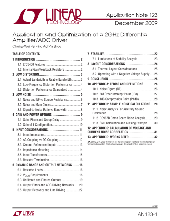
TABLE OF CONTENTS 7 STABILITY ............................................... 1 INTRODUCTION .......................................... 7.1 Limitations of Stability Analysis .....................23 1.1 LTC6400 Features ............................................2 8 LAYOUT CONSIDERATIONS ........................... 1.2 Internal Gain/Feedback Resistors ....................2 8.1 Thermal Layout Considerations .....................25 2 LOW DISTORTION....................................... 8.2 Operating with a Negative Voltage Supply .....25 2.1 Actual Bandwidth vs Usable Bandwidth ...........3 9 CONCLUSION ........................................... 2.2 Low-Frequency Distortion Performance ..........4 10 APPENDIX A: TERMS AND DEFINITIONS .......... 2.3 Distortion Performance Guaranteed ................4 10.1 Noise Figure (NF) .........................................26 3 LOW NOISE .............................................. 10.2 3rd Order Intercept Point (IP3) ....................27 3.1 Noise and NF vs Source Resistance .................6 10.3 1d B Compression Point (P1d B) ...................28 3.2 Noise and Gain Circles .....................................7 11 APPENDIX B: SAMPLE NOISE CALCULATIONS ... 3.3 Signal-to-Noise Ratio vs Bandwidth ................8 11.1 Noise Analysis For Arbitrary Source Resistance ............................................................28

4 GAIN AND POWER OPTIONS ..........................

11.2 DC987B Demo Board Noise Analysis ...........29

4.1 Gain, Phase and Group Delay ..........................9

11.3 SNR Calculation and Aliasing Example ........30

4.2 Gain of 1 Confi guration ..................................10

12 APPENDIX C: CALCULATION OF VOLTAGE AND

5 INPUT CONSIDERATIONS .............................

CURRENT NOISE CORRELATION ........................

5.1 Input Impedance ............................................11

13 APPENDIX D: WORKS CITED ........................

5.2 AC Coupling vs DC Coupling ..........................12

L, LT, LTC, LTM, Linear Technology and the Linear logo are registered trademarks of Linear Technology Corporation. All other trademarks are the property of their respective owners.

5.3 Ground-Referenced Inputs ............................13 5.4 Impedance Matching .....................................14 5.5 Input Transformers ........................................15 5.6 Resistor Termination......................................16 6 DYNAMIC RANGE AND OUTPUT NETWORKS ...... 6.1 Resistive Loads .............................................18 6.2 VOCM Requirements .......................................18 6.3 Unfi ltered and Filtered Outputs ......................19 6.4 Output Filters and ADC Driving Networks ......20 6.5 Output Recovery and Line Driving .................22

an123f

AN123-1

Page Summary Contents For LINEAR Application Note AN123: Application and Optimization of a 2GHz Differential Amplifier ADC Driver Manual User Guide

Page 1 Application Note 123 December 2009 Application and Optimization of a 2GHz Differential Amplifi er/ADC Driver Cheng-Wei Pei and Adam Shou TABLE OF CONTENTS 7 STABILITY ....................................
Page 2 Application Note 123 1 INTRODUCTION family is unconditionally stable with any input and output termination, and in fact the output does not require any Modern high speed analog-to-digital converters (...
Page 3 Application Note 123 LBOND1 V– ENABLE V+ V– LBOND3 BIAS CONTROL 12.5Ω CPAR3 RG RF ROUT LBOND4 100Ω 500Ω 12.5Ω 12.5Ω +IN +OUT CPAR4 RFILT LBOND2 50Ω R4R3 +OUTF +IN IN+ OUT– CFILT AN123 F1-2 RFILT 1.7p ...
Page 4 Application Note 123 IR c) Figure 2-2 shows the 3rd order intermodulation distor- systems to provide gain with no measurable degradation tion (IMD) products from a 2-tone signal test of the in the sig...
Page 5 Application Note 123 Table 2-1. Typical and Guaranteed 2-Tone 3rd Order IMD RI1 RF1 Specifi cations for the LTC6400 Family of Products. These Specifi cations are Measured and Guaranteed at Room Temper...
Page 6 Application Note 123 Table 3-1: Equivalent Input and Output Noise at 100MHz Based RS = 0Ω on the Internal Noise Sources in Figure 3-1. The First Two Rows, NO RL en and in, are Calculated Input-Referre...
Page 7 Application Note 123 (d (see Appendix A). Also, the noise fi gure curves shown in RS = 0Ω, NO RL Figure 3-4 are not monotonic as RS increases, but instead MEASURED AT 100MHz LTC6400-8 have a local min...
Page 8 Application Note 123 a signifi cant portion of the real axis available (including Table 3-2. LTC6400 Complex Noise Parameters Measured at 100MHz. These Parameters are the Basis for the Noise Figure 40...
Page 9 Application Note 123 multiplying the noise voltage density by the square root digital fi ltering to improve the SNR. If all of the noise is of the total bandwidth. contained in one Nyquist bandwidth (...
Page 10 Application Note 123 V– ENABLE V+ V– BIAS CONTROL ROUT VOLTAGE GAIN IN RG RF (n s) RG 12.5ΩRF +IN +OUT 8d B 200Ω 500Ω 14d B 100Ω 500Ω 20d B 100Ω 1kΩ RFILT 50Ω +OUTF +IN IN+ OUT– CFILT INPUT FREQUENCY ...
Page 11 Application Note 123 When combining external series resistors to lower the RI1 RF1 INT+ gain, there will be some temperature and initial accuracy limitations due to the characteristics of the LTC6400 ...
Page 12 Application Note 123 seen by VIN in the example. Note that in the case of a VIN and the resultant internal node voltages (see Figure 5-1) with non-zero source impedance, such as a 50Ω signal that resu...
Page 13 Application Note 123 When calculating the input minimum and maximum volt- 75Ω resistors to the supply. This circuit takes advantage ages with the provided equations, it is important to keep of the sou...
Page 14 Application Note 123 R1 RI1 RF1 RO1 RI RF RT VIN LTC6400-8 LTC6400-20 50Ω R2 RI2 RF2 RO2 RI RF 1100Ω 200Ω 500Ω 12.5Ω 100Ω 1000Ω AN123 F5-4 Figure 5-4. Use Two LTC6400 Amplifi ers to Level Shift and Am...
Page 15 Application Note 123 LTC6400-14 LTC6400-8 LTC6400-20 INPUT INPUT LTC6400 UNFILTERED OUTPUT Figure 5-7. Differential Input and Output Impedance Matching Figure 5-9. Output Refl ection Coeffi cients (S2...
Page 16 Application Note 123 VCC VCC DIS R16 0Ω C17 C18 JP1 1000p F 0.1μF EN R14 VEEC VCCB VEEBEN T1 R4 C21 +INB +OUT T2 +IN +OUT (2) (2)15 0.1μF R8 (1) TCM 4-19 +INA +OUTF R7 (1) C3 SL2 (2)SL1 (2) –INB –OUTF...
Page 17 Application Note 123 impedance match than even the best RF transformers, RI1 RF1 SOURCE and the frequency response of resistors extends down to 200Ω 500Ω DC. There is a penalty to pay in noise fi gure...
Page 18 Application Note 123 In Equations 5-6 and 5-7, RI and RF are the values of the –40 DIFFERENTIAL INPUT VOUT = 2VP-P internal gain and feedback resistors, 200Ω and 500Ω respectively in Figure 5-12. Tabl...
Page 19 Application Note 123 –80 –80 LTC6400-8 LTC6400-14 IM c) IM c) COMMON MODE VOLTAGE (V) COMMON MODE VOLTAGE (V) –80 –80 LTC6400-20 LTC6400-26 IM c) IM c) COMMON MODE VOLTAGE (V) COMMON MODE VOLTAGE (V) ...
Page 20 Application Note 123 6.4 Output Filters and ADC Driving Networks The LTC6400 by itself does have low output impedance and the ability to settle relatively quickly after a charge injection It is often ...
Page 21 Application Note 123 The size of R1 and R2 is not largely constrained, except the passband of the RLC fi lter, the network will not attenu- for in the case of lower frequency cutoff fi lters. If the t...
Page 22 Application Note 123 IO s) 6.5 Output Recovery and Line Driving the propagation delay remains less than 3ns. Figure 6-8 is a schematic of the circuit used to measure the data in Many feedback amplifi ...
Page 23 Application Note 123 7.1 Limitations of Stability Analysis Another limitation of this stability calculation method is that the S-parameters are made with symmetrical inputs The measurements for Figure...
Page 24 Application Note 123 8 LAYOUT CONSIDERATIONS located on opposite sides of the chip, and the power and control pins are located on the remaining two sides. This The LTC6400 is a high speed fully differ...
Page 25 Application Note 123 8.2 Operating with a Negative Voltage Supply In certain situations, it may be desirable to operate the LTC6400 with a V– supply that is not the board ground. For example, if opera...
Page 26 Application Note 123 INPUTS OUTPUTS PIN 1 Figure 8-3. Sample Top Layer (8-3a) and Bottom Layer (8-3b) Layout with Dual Voltage Supplies. All Power Supply Bypass Capacitors are Labeled as CBYP 9 CONCLU...
Page 27 Application Note 123 from the resistive part of the source impedance ZS, as ideal closest tones are the 3rd order intermodulation distortion capacitors and inductors are noiseless. So substituting RS ...
Page 28 Application Note 123 load at all. This leads us to defi ne an equivalent output until the amplifi er’s output is actually saturated. So the power level, which uses the voltage-swing equivalence signal...
Page 29 Application Note 123 •= i N +2 β• 2β n V( Hz( (11-1) OUT F( FR where: 11.2 DC987B Demo Board Noise Analysis β = 4k T = 1.6008 • 10–20 (J), RF = RF1 = RF2 (Ω), This section extends the noise calculatio...
Page 30 Application Note 123 To apply the formula, translate the decibel NFs back to 11.3 SNR Calculation and Aliasing Example the linear noise factor (F). In our case, 6.14d B becomes This example attempts t...
Page 31 Application Note 123 the same as the ADC’s SNR, the amplifi er needs to have SNRLIN =10 lower output noise density and/or lower bandwidth. The preceding analysis and Figure 11-3 assume the alias NOISE...
Page 32 Application Note 123 should be some level of correlation between the two. If cancelling the voltage noise (depending on the phase of there is signifi cant correlation, then it should be possible inc •...

Manual Details

Brand Linear
Pages 32
File Size 524.75 KB
Published June 17, 2026
8 views

Enter the captcha to get the download link:

captcha

Frequently Asked Questions

Is the LTC6400 unconditionally stable?

Yes, the family is unconditionally stable with any input and output termination.

Does the ADC driver need impedance-matching components?

No, modern high speed analog-to-digital converters (ADC), like those in the LTC6400 family, do not require impedance-matching components when driving an ADC.

What is an advantage of internal gain resistors?

Internal gain/feedback resistors allow the front end to contain sensitive feedback loop nodes within the chip, making the design simpler and less susceptible to parasitic PCB capacitances compared to external differential amplifiers.

How does output filtering affect the overall solution?

Output filters and ADC driving networks enable wider signal bandwidths and relax the performance requirements for analog anti-alias filtering.