Fairchild Power MOSFETs and their Applications User Manual
Summary
Discover foundational knowledge on Power MOSFETs, advanced voltage-controlled switches designed for high-power circuit applications. This guide details MOSFET operation, comparing traditional lateral designs with superior vertical DMOS structures. Learn about key technical characteristics, including fast switching speeds, low gate power requirements, and structural considerations needed to optimize your device performance. Essential reading for engineers designing effective electrical switching systems.
Page 1 Text Content
Application Note 558 Ralph Locher
Introduction to Power MOSFETs and their Applications INTRODUCTION
The Power MOSFETs that are available today perform the same function as Bipolar transistors except the former are voltage controlled in contrast to the current controlled Bipolar devices. Today MOSFETs owe their ever-increasing popularity to their high input impedance and to the fact that being a majority carrier device, they do not suffer from minority carrier storage time effects, ther- mal runaway, or second breakdown.
MOSFET OPERATION
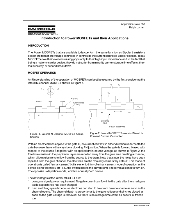
An Understanding of the operation of MOSFETs can best be gleaned by the first considering the lateral N-channel MOSFET shown in Figure 1.
METAL (AL)
SOURCE GATE DRAIN
SILICON DIOXIDE (Si O )2
Si O2
INVERTED ZONE
P BODY SUBSTRATE
Figure 2. Lateral MOSFET Transistor Biased for
Figure 1. Lateral N-Channel MOSFET Cross-
Forward Current Conduction
Section
With no electrical bias applied to the gate G, no current can flow in either direction underneath the gate because there will always be a blocking PN junction. When the gate is forward biased with respect to the source S together with an applied drain-source voltage, as shown in Figure 2, the free hole carriers in the p-epitaxial layer are repelled away from the gate area creating a channel, which allows electrons to flow from the source to the drain. Note that since the holes have been repelled from the gate channel, the electrons are the “majority carriers” by default. This mode of operation is called “enhancement” but is easier to think of enhancement mode of operation as the device being “normally off”, i.e., the switch blocks the current until it receives a signal to turn on. The opposite is depletion mode, which is normally “on” device.
The advantages of the lateral MOSFET are: 1. Low gate signal power requirement. No gate current can flow into the gate after the small gate oxide capacitance has been charged. 2. Fast switching speeds because electrons can start to flow from drain to source as soon as the channel opens. The channel depth is proportional to the gate voltage and pinches closed as soon as the gate voltage is removed, so there is no storage time effect as occurs in transis tors.
Rev B, October 1998
Page Summary Contents For Fairchild Power MOSFETs and their Applications User Manual
Manual Details
| Brand | Fairchild |
|---|---|
| Pages | 15 |
| File Size | 200.61 KB |
| Published | June 16, 2026 |
Enter the captcha to get the download link:

Frequently Asked Questions
How are MOSFETs different from Bipolar transistors?
MOSFETs are voltage controlled, unlike current-controlled Bipolar devices, and they feature high input impedance.
What improvement does the vertical DMOS structure provide?
Vertical geometry allows for lower on-state resistance (Rds(on)) and faster switching than lateral MOSFETs.
What is the limitation of standard lateral MOSFETs?
The channel length cannot be shorter than the minimum depletion width required to support the device's rated voltage.
Are these components safe for life support applications?
No, they are not authorized for critical use in life support devices without express written approval from Fairchild Semiconductor Corporation.