Fairchild SuperSOT -3 Power MOSFETs Data Handbook
Summary
Optimize power handling in space-constrained designs using this detailed guide on the SuperSOT-3 Power MOSFET. The manual provides essential technical knowledge for circuit board designers working in high-density power electronics, focusing specifically on maximizing thermal performance through optimal copper mounting pad layout. It analyzes the theory of heat dissipation and demonstrates how precise design considerations can significantly lower junction-to-ambient thermal resistance, ensuring reliable operation even with minimized cooling space.
Page 1 Text Content
AN1025 April, 1996
Maximum Power Enhancement Techniques for Super SOTTM-3 Power MOSFETs
Alan Li, Brij Mohan, Steve Sapp, Izak Bencuya, Linh Hong
1. Introduction
As packages become smaller, achieving efficient thermal performance for power applications requires that the designers employ new methods of meliorating the heat flow out of devices. Thus the purpose of this paper is to aid the user in maximizing the power handling capability of the Super SOTTM-3 (SOT-23) Power MOSFET offered by Fairchild Semiconductor. This effort allows the user to take full advantage of the exceptional performance features of Fairchild’s state-of-the-art Power MOSFET which offers very low on-resistance and improved junction-to- case (RθJC ) thermal resistance. Ultimately the user may achieve improved component perfor- mance and higher circuit board packing density by using the thermal solution suggested below.
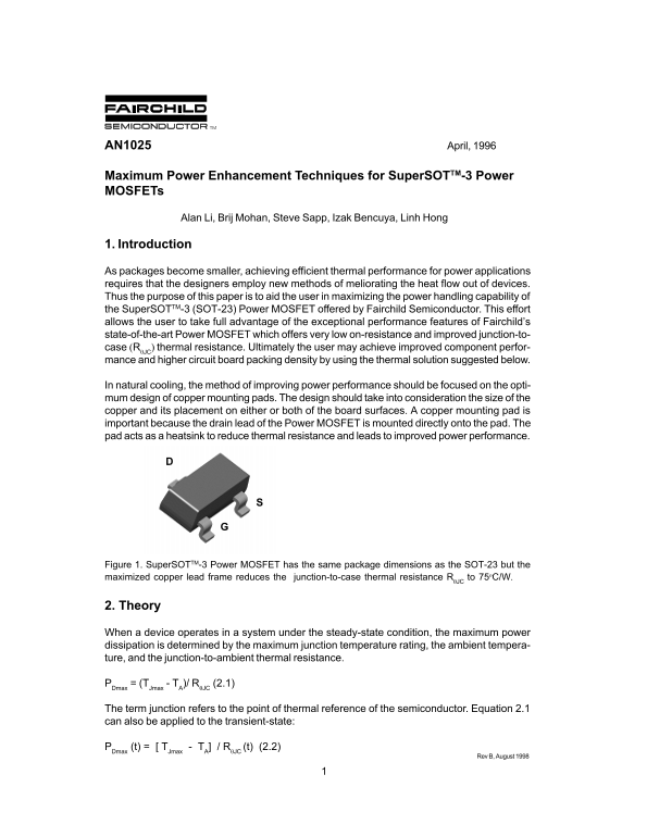
In natural cooling, the method of improving power performance should be focused on the opti- mum design of copper mounting pads. The design should take into consideration the size of the copper and its placement on either or both of the board surfaces. A copper mounting pad is important because the drain lead of the Power MOSFET is mounted directly onto the pad. The pad acts as a heatsink to reduce thermal resistance and leads to improved power performance.
Figure 1. Super SOTTM-3 Power MOSFET has the same package dimensions as the SOT-23 but the maximized copper lead frame reduces the junction-to-case thermal resistance RθJC to 75o C/W.
2. Theory
When a device operates in a system under the steady-state condition, the maximum power dissipation is determined by the maximum junction temperature rating, the ambient tempera- ture, and the junction-to-ambient thermal resistance.
= (T - T )/ RθJC (2.1) Dmax Jmax
The term junction refers to the point of thermal reference of the semiconductor. Equation 2.1 can also be applied to the transient-state:
(t) = [ T - T ] / RθJC (t) (2.2) Dmax Jmax
Rev B, August 1998
Page Summary Contents For Fairchild SuperSOT -3 Power MOSFETs Data Handbook
Manual Details
| Brand | Fairchild |
|---|---|
| Pages | 11 |
| File Size | 254.29 KB |
| Published | June 20, 2026 |
Enter the captcha to get the download link:
