Fairchild 74VHC125 Quad Buffer with 3-STATE Outputs Data Handbook
Summary
This advanced quad buffer features four independent non-inverting buffers with robust 3-STATE outputs. Designed for reliable system interfacing, it is ideal for developers working on mixed-voltage environments, such as connecting 5V to 3V systems or implementing battery backup architectures. The device offers high speed, low power consumption, and critical Power-Down protection against mismatched supply voltages. The accompanying manual provides comprehensive details including full electrical characteristics, operating conditions, pin mappings, and application guidelines necessary for robust signal conditioning in professional electronic designs.
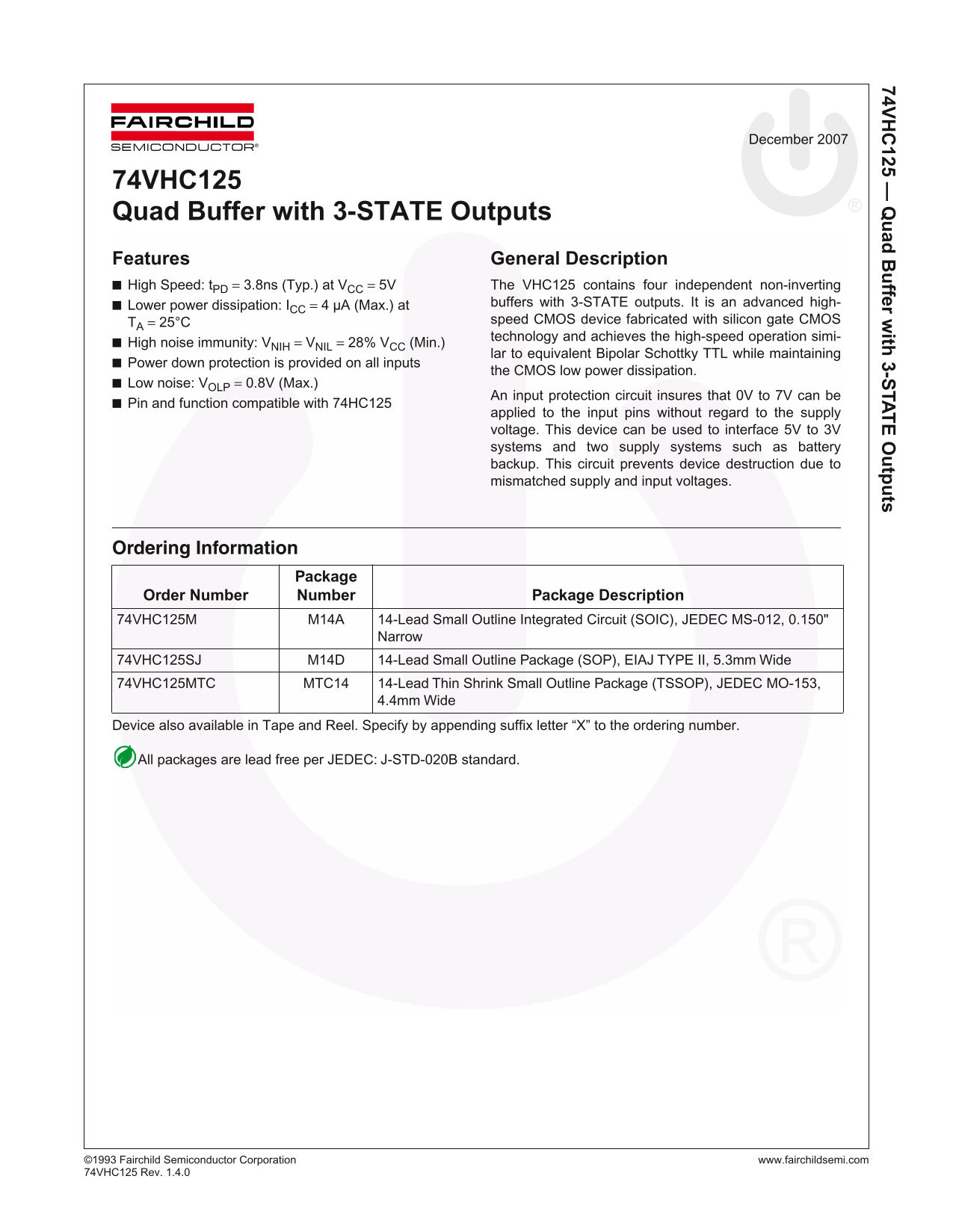
Page 1 Text Content
74V 125 — ad ffer w ith 3-S TA tp ts
December 2007
74VHC125 Quad Buffer with 3-STATE Outputs Features General Description High Speed: t PD = 3.8ns (Typ.) at VCC = 5V The VHC125 contains four independent non-inverting
Lower power dissipation: ICC = 4 µA (Max.) at buffers with 3-STATE outputs. It is an advanced high- TA = 25°C speed CMOS device fabricated with silicon gate CMOS technology and achieves the high-speed operation simi-
High noise immunity: VNIH = VNIL = 28% VCC (Min.)
lar to equivalent Bipolar Schottky TTL while maintaining
Power down protection is provided on all inputs
the CMOS low power dissipation.
Low noise: VOLP = 0.8V (Max.)
An input protection circuit insures that 0V to 7V can be
Pin and function compatible with 74HC125
applied to the input pins without regard to the supply voltage. This device can be used to interface 5V to 3V systems and two supply systems such as battery backup. This circuit prevents device destruction due to mismatched supply and input voltages.
Ordering Information
Package
Order Number Number Package Description 74VHC125M M14A 14-Lead Small Outline Integrated Circuit (SOIC), JEDEC MS-012, 0.150"
Narrow
74VHC125SJ M14D 14-Lead Small Outline Package (SOP), EIAJ TYPE II, 5.3mm Wide 74VHC125MTC MTC14 14-Lead Thin Shrink Small Outline Package (TSSOP), JEDEC MO-153,
4.4mm Wide
Device also available in Tape and Reel. Specify by appending suffix letter “X” to the ordering number.
All packages are lead free per JEDEC: J-STD-020B standard.
©1 993 Fairchild Semiconductor Corporation www.fairchildsemi.com 74V HC125 Rev. 1.4.0
Page Summary Contents For Fairchild 74VHC125 Quad Buffer with 3-STATE Outputs Data Handbook
Manual Details
| Brand | Fairchild |
|---|---|
| Pages | 9 |
| File Size | 289.13 KB |
| Published | July 06, 2026 |
Enter the captcha to get the download link:

Frequently Asked Questions
Can the 74VHC125 interface between different supply voltages?
Yes, it can be used to interface systems from 5V down to 3V, or two-supply systems like battery backup.
What is required for unconnected input pins before use?
Unused inputs must be actively held either HIGH or LOW; they cannot float.
How are the device's absolute maximum ratings different from recommended operating conditions?
Absolute maximum ratings only indicate stress limits. Recommended operating conditions define parameters for optimal performance and safe design.
What is the typical operational speed of this high-speed buffer module?
The delay time (t) is typically 3.8ns when operating at a 5V supply voltage.