Fairchild NC7WP240 TinyLogic ULP Dual Inverting Buffer with 3-STATE Outputs - Data Sheet
Summary
A datasheet for the NC7WP240 TinyLogic ULP dual inverting buffer with 3-STATE outputs from Fairchild Semiconductor. The device features ultra-low power consumption, 0.9V to 3.6V supply operation, 3.6V overvoltage tolerant I/Os, and typical propagation delays from 3ns to 26ns across voltage ranges. Available in US8 and MicroPak leadless packages, it includes patented Quiet Series noise/EMI reduction circuitry and power-off high impedance protection. The manual covers functional description, electrical characteristics, timing parameters, and ordering information. Targeted at portable electronics designers prioritizing battery life and board space savings.
Page 1 Text Content
7W 240 T in y L ic al In vertin ffer w ith 3-S TA tp ts
June 2003 Revised January 2005
NC7WP240 Tiny Logic ULP Dual Inverting Buffer with 3-STATE Outputs General Description Features The NC7WP240 is a Dual Inverting Buffer with indepen- ■Space saving US8 surface mount package dent active LOW enables for the 3-STATE outputs. The ■Micro Pak Pb-Free leadless package Ultra High Power device is ideal for applications where bat-
■0.9V to 3.6V VCC supply operation
tery life is critical. This product is designed for ultra low
power consumption within the VCC operating range of 0.9V ■3.6V overvoltage tolerant I/O’s at VCC from 0.9V to 3.6V
to 3.6V VCC. t PD The internal circuit is composed of a minimum of inverter 3.0 ns typ for 3.6V VCC stages, including the output buffer, to enable ultra low static
4.0 ns typ for 2.3V to 2.7V VCC
and dynamic power.
5.0 ns typ for 1.65V to 1.95V VCC
The NC7WP240 for lower drive requirements, is uniquely designed for optimized power and speed, and is fabricated 6.0 ns typ for 1.40V to 1.60V VCC with an advanced CMOS technology to achieve best in
10.0 ns typ for 1.10V to 1.30V VCC
class speed operation while maintaining extremely low
CMOS power dissipation. 26.0 ns typ for 0.90V VCC ■Power-Off high impedance inputs and outputs ■Static Drive (IOH/IOL) ±2.6 m A @ 3.00V VCC ±2.1 m A @ 2.30V VCC ±1.5 m A @ 1.65V VCC ±1.0 m A @ 1.40V VCC ±0.5 m A @ 1.10V VCC ±20 µA @ 0.9V VCC ■Uses patented Quiet Series noise/EMI reduction circuitry ■Ultra low dynamic power
Ordering Code:
Product Package Code Package Description Supplied As Order
Number Number Top Mark NC7WP240K8X MAB08A WP40 8-Lead US8, JEDEC MO-187, Variation CA 3.1mm Wide 3k Units on Tape and Reel NC7WP240L8X MAC08A Z3 Pb-Free 8-Lead Micro Pak, 1.6 mm Wide 5k Units on Tape and Reel Pb-Free package per JEDEC J-STD-020B.
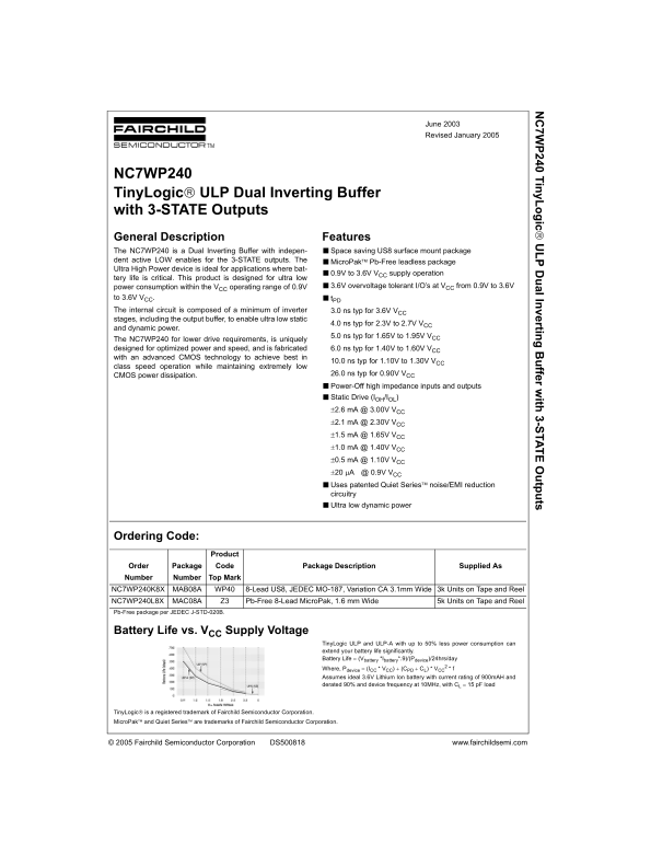
Battery Life vs. VCC Supply Voltage
Tiny Logic ULP and ULP-A with up to 50% less power consumption can extend your battery life significantly. Battery Life = (Vbattery *Ibattery*.9)/(Pdevice)/24hrs/day
Where, Pdevice = (ICC * VCC) + (CPD + CL) * VCC Assumes ideal 3.6V Lithium Ion battery with current rating of 900m AH and derated 90% and device frequency at 10MHz, with CL = 15 p F load
Tiny Logic is a registered trademark of Fairchild Semiconductor Corporation. Micro Pak and Quiet Series are trademarks of Fairchild Semiconductor Corporation.
© 2005 Fairchild Semiconductor Corporation DS500818 www.fairchildsemi.com
Page Summary Contents For Fairchild NC7WP240 TinyLogic ULP Dual Inverting Buffer with 3-STATE Outputs - Data Sheet
Manual Details
| Brand | Fairchild |
|---|---|
| Pages | 10 |
| File Size | 209.03 KB |
| Published | June 17, 2026 |
Enter the captcha to get the download link:

Frequently Asked Questions
What is the operating voltage range for the NC7WP240?
The device operates with a V_CC supply from 0.9V to 3.6V.
What packages are available for the NC7WP240?
It is available in an 8-Lead US8 surface mount package and an 8-Lead MicroPak leadless package.
What are the typical propagation delay times?
Typical delays range from 3.0 ns at 3.6V V_CC to 26.0 ns at 0.9V V_CC, varying by supply voltage.
What is the purpose of the OE (Output Enable) pin?
The OE pin is an active LOW enable that controls the 3-STATE outputs, placing them in a high-impedance (Z) state when HIGH.