Fairchild FAN4800 Combo Controller Applications Manual
Summary
Design reliable, high-performance AC/DC regulated power supplies with the FAN4800 Combo Controller. This application note provides comprehensive, step-by-step engineering guidance for implementing the PFC stage, ensuring compliant and efficient operation across wide input voltages (85V-265V). Ideal for electrical engineers designing robust systems requiring stable output voltage and maximizing power availability.
Page 1 Text Content
www.fairchildsemi.com
Application Note AN6032 FAN4800 Combo Controller Applications General Description The PFC Stage This application note shows the step-by-step process to
Powering the FAN4800
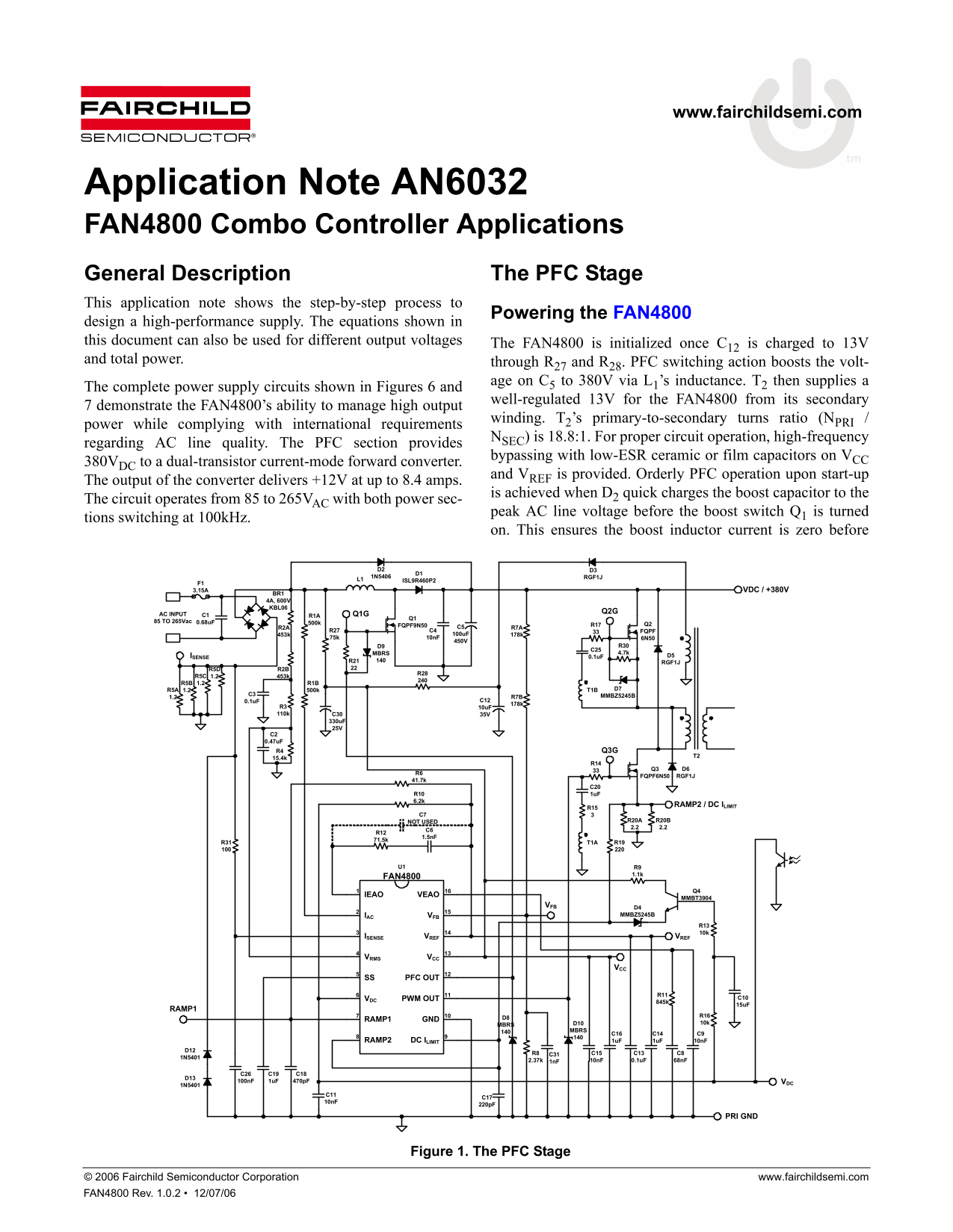
design a high-performance supply. The equations shown in this document can also be used for different output voltages The FAN4800 is initialized once C12 is charged to 13V and total power. through R27 and R28. PFC switching action boosts the volt-
age on C5 to 380V via L1’s inductance. T2 then supplies a
The complete power supply circuits shown in Figures 6 and
well-regulated 13V for the FAN4800 from its secondary
7 demonstrate the FAN4800’s ability to manage high output
winding. T2’s primary-to-secondary turns ratio (NPRI /
power while complying with international requirements
NSEC) is 18.8:1. For proper circuit operation, high-frequency
regarding AC line quality. The PFC section provides
bypassing with low-ESR ceramic or film capacitors on VCC
380VDC to a dual-transistor current-mode forward converter.
and VREF is provided. Orderly PFC operation upon start-up
The output of the converter delivers +12V at up to 8.4 amps.
is achieved when D2 quick charges the boost capacitor to the
The circuit operates from 85 to 265VAC with both power sec-
peak AC line voltage before the boost switch Q1 is turned
tions switching at 100k Hz.
on. This ensures the boost inductor current is zero before
L1 RGF1J
F1 ISL9R460P2
3.15A VDC / +380V
BR1 4A, 600V KBL06
AC INPUT Q1G Q2G
85 TO 265Vac Q1
R2A FQPF9N50 C5 R7A
R27 C4 FQPF
ISENSE MBRS D5
R21 RGF1J
1.2 C3 R7B MMBZ5245B
R6 FQPF6N50 RGF1J 41.7k
R15 RAMP2 / DC ILIMIT
NOT USED R20A R20B C6 2.2 2.2
FAN4800 1.1k
IEAO VEAO MMBT3904
VFB D4
IAC VFB MMBZ5245B
ISENSE VREF VREF
VRMS VCC
SS PFC OUT
VDC PWM OUT 845k
RAMP1
RAMP1 GND 10k
MBRS D10 MBRS
RAMP2 DC ILIMIT 1u F 1u F 10n F
1N5401 VDC
PRI GND
Figure 1. The PFC Stage
© 2006 Fairchild Semiconductor Corporation www.fairchildsemi.com FAN4800 Rev. 1.0.2 • 12/07/06
Page Summary Contents For Fairchild FAN4800 Combo Controller Applications Manual
Manual Details
| Brand | Fairchild |
|---|---|
| Pages | 10 |
| File Size | 453.82 KB |
| Published | July 06, 2026 |
Enter the captcha to get the download link:
