Fairchild NC7WZ16 TinyLogic UHS Dual Buffer Data Handbook
Summary
This ultra-high speed dual buffer is engineered for reliable signal translation across broad voltage ranges (1.65V to 5.5V). Designed with advanced CMOS technology, it features high output drive capability and low power dissipation. This comprehensive manual provides electrical specifications, absolute maximum ratings, detailed pin configurations, and application guidelines required by hardware designers implementing high-performance logic circuits.
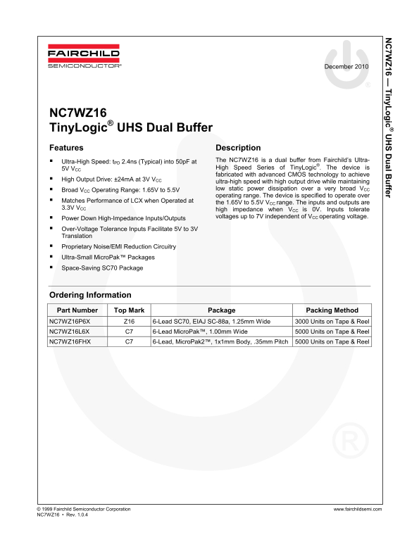
Page 1 Text Content
7W Z16 — Tiny Logic S D ual B uffer
December 2010
NC7WZ16 Tiny Logic® UHS Dual Buffer Features Description
Ultra-High Speed: t PD 2.4ns (Typical) into 50p F at The NC7WZ16 is a dual buffer from Fairchild’s Ultra- 5V VCC High Speed Series of Tiny Logic®. The device is fabricated with advanced CMOS technology to achieve
High Output Drive: ±24m A at 3V VCC
ultra-high speed with high output drive while maintaining Broad VCC Operating Range: 1.65V to 5.5V low static power dissipation over a very broad VCC operating range. The device is specified to operate over
Matches Performance of LCX when Operated at
the 1.65V to 5.5V VCC range. The inputs and outputs are
3.3V VCC
high impedance when VCC is 0V. Inputs tolerate Power Down High-Impedance Inputs/Outputs voltages up to 7V independent of VCC operating voltage.
Over-Voltage Tolerance Inputs Facilitate 5V to 3V Translation Proprietary Noise/EMI Reduction Circuitry Ultra-Small Micro Pak™ Packages Space-Saving SC70 Package
Ordering Information Part Number Top Mark Package Packing Method NC7WZ16P6X Z16 6-Lead SC70, EIAJ SC-88a, 1.25mm Wide 3000 Units on Tape & Reel NC7WZ16L6X C7 6-Lead Micro Pak™, 1.00mm Wide 5000 Units on Tape & Reel NC7WZ16FHX C7 6-Lead, Micro Pak2™, 1x1mm Body, .35mm Pitch 5000 Units on Tape & Reel
© 1999 Fairchild Semiconductor Corporation www.fairchildsemi.com NC7WZ16 • Rev. 1.0.4
Page Summary Contents For Fairchild NC7WZ16 TinyLogic UHS Dual Buffer Data Handbook
Manual Details
| Brand | Fairchild |
|---|---|
| Pages | 9 |
| File Size | 529.02 KB |
| Published | June 03, 2026 |
Enter the captcha to get the download link:

Frequently Asked Questions
What is the recommended operating temperature range for this device?
The unit operates within a temperature range of -40°C to +125°C.
How can I safely connect external signals if they exceed the supply voltage?
Inputs tolerate voltages up to 7V, regardless of the operational VCC.
What is the characteristic speed of the NC7WZ16 dual buffer?
It provides ultra-high speed with a typical time constant (t) of 2.4ns into 50pF.
On the SC70 package, which pin functions as ground?
Pin #2 is designated for Ground (GND).