Fairchild NC7WZU04 TinyLogic UHS Dual Unbuffered Inverter Data Handbook
Summary
Designed for high-speed digital applications, this dual unbuffered inverter offers reliable signal handling across a broad operating voltage range (1.65V to 5.5V). Utilizing advanced CMOS technology in compact SC70 or MicroPak packages, the unit delivers exceptional stability and ultra-low quiescent power ideal for crystal oscillator and general analog circuits. This comprehensive manual provides engineers with detailed pin assignments, electrical characteristics, absolute maximum ratings, and performance guidelines necessary for precise system integration and optimal circuit design.
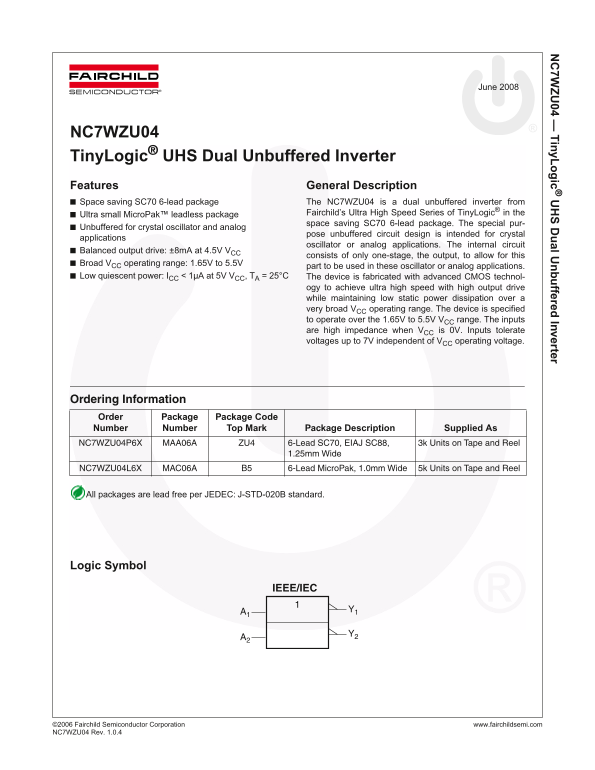
Page 1 Text Content
7W 04 — iny L ic al U bu ffered Inverter
June 2008
NC7WZU04 Tiny Logic® UHS Dual Unbuffered Inverter Features General Description Space saving SC70 6-lead package The NC7WZU04 is a dual unbuffered inverter from
Ultra small Micro Pak™ leadless package Fairchild’s Ultra High Speed Series of Tiny Logic® in the space saving SC70 6-lead package. The special pur-
Unbuffered for crystal oscillator and analog
pose unbuffered circuit design is intended for crystal
applications
oscillator or analog applications. The internal circuit
Balanced output drive: ±8m A at 4.5V VCC
consists of only one-stage, the output, to allow for this
Broad VCC operating range: 1.65V to 5.5V
part to be used in these oscillator or analog applications.
Low quiescent power: ICC < 1µA at 5V VCC, TA = 25°C The device is fabricated with advanced CMOS technol-
ogy to achieve ultra high speed with high output drive while maintaining low static power dissipation over a very broad VCC operating range. The device is specified to operate over the 1.65V to 5.5V VCC range. The inputs are high impedance when VCC is 0V. Inputs tolerate voltages up to 7V independent of VCC operating voltage.
Ordering Information Order Package Package Code Number Number Top Mark Package Description Supplied As NC7WZU04P6X MAA06A ZU4 6-Lead SC70, EIAJ SC88, 3k Units on Tape and Reel
1.25mm Wide
NC7WZU04L6X MAC06A B5 6-Lead Micro Pak, 1.0mm Wide 5k Units on Tape and Reel
All packages are lead free per JEDEC: J-STD-020B standard.
Logic Symbol
IEEE/IEC
©2 006 Fairchild Semiconductor Corporation www.fairchildsemi.com NC 7WZU04 Rev. 1.0.4
Page Summary Contents For Fairchild NC7WZU04 TinyLogic UHS Dual Unbuffered Inverter Data Handbook
Manual Details
| Brand | Fairchild |
|---|---|
| Pages | 11 |
| File Size | 361.35 KB |
| Published | May 31, 2026 |
Enter the captcha to get the download link:

Frequently Asked Questions
What operating voltage range is recommended for the device?
The device should operate in a supply voltage (V CC) range of 1.8V to 5.5V.
Can this inverter be used with crystal oscillators or analog circuits?
Yes, its unbuffered circuit design makes it suitable for both crystal oscillator and analog applications.
How can I determine the Pin One location on the package?
Read the top product code mark from left to right; Pin One is located at the lower left pin.
What are the power dissipation limits?
The maximum power dissipation is 215mW for both SC70-6 and MicroPak-6 packages.